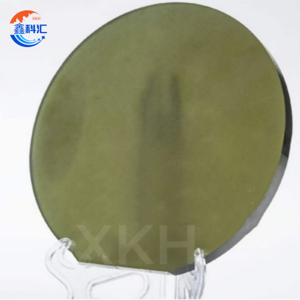
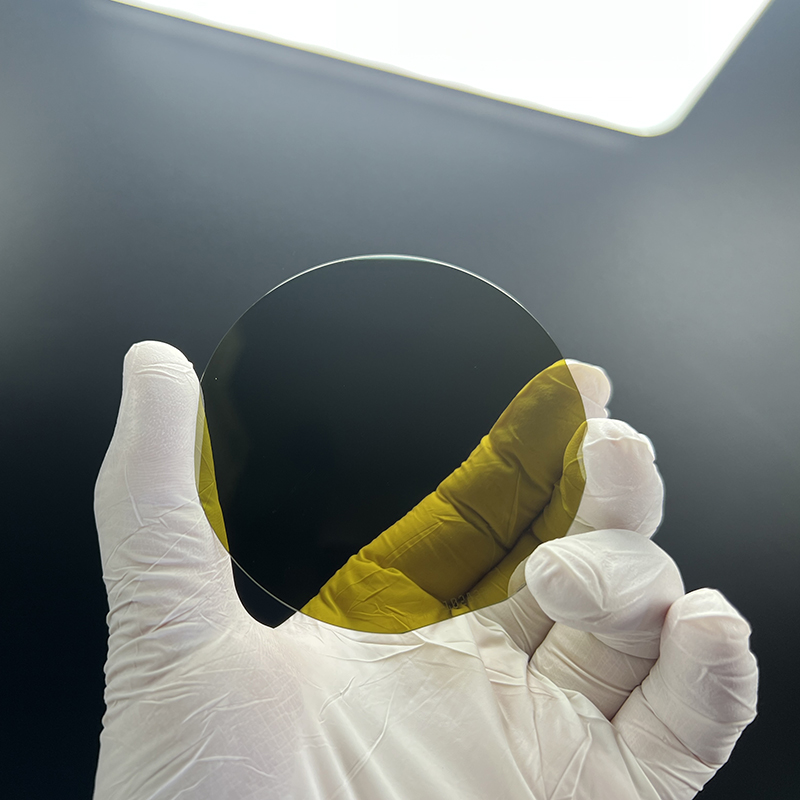
12 inch SIC substrate silicon carbide prime grade diameter 300mm large size 4H-N Suitable for high power device heat dissipation


Product characteristics
1. High thermal conductivity: the thermal conductivity of silicon carbide is more than 3 times that of silicon, which is suitable for high power device heat dissipation.
2. High breakdown field strength: The breakdown field strength is 10 times that of silicon, suitable for high-pressure applications.
3.Wide bandgap: The bandgap is 3.26eV (4H-SiC), suitable for high temperature and high frequency applications.
4. High hardness: Mohs hardness is 9.2, second only to diamond, excellent wear resistance and mechanical strength.
5. Chemical stability: strong corrosion resistance, stable performance in high temperature and harsh environment.
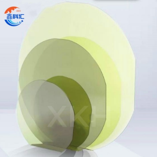
6. Large size: 12 inch (300mm) substrate, improve production efficiency, reduce unit cost.
7.Low defect density: high quality single crystal growth technology to ensure low defect density and high consistency.
Product main application direction
1. Power electronics:
Mosfets: Used in electric vehicles, industrial motor drives and power converters.
Diodes: such as Schottky diodes (SBD), used for efficient rectification and switching power supplies.
2. Rf devices:
Rf power amplifier: used in 5G communication base stations and satellite communications.
Microwave devices: Suitable for radar and wireless communication systems.
3. New energy vehicles:
Electric drive systems: motor controllers and inverters for electric vehicles.
Charging pile: Power module for fast charging equipment.
4. Industrial applications:
High voltage inverter: for industrial motor control and energy management.
Smart grid: For HVDC transmission and power electronics transformers.
5. Aerospace:
High temperature electronics: suitable for high temperature environments of aerospace equipment.
6. Research field:
Wide bandgap semiconductor research: for the development of new semiconductor materials and devices.
The 12-inch silicon carbide substrate is a kind of high-performance semiconductor material substrate with excellent properties such as high thermal conductivity, high breakdown field strength and wide band gap. It is widely used in power electronics, radio frequency devices, new energy vehicles, industrial control and aerospace, and is a key material to promote the development of the next generation of efficient and high-power electronic devices.
While silicon carbide substrates currently have fewer direct applications in consumer electronics such as AR glasses, their potential in efficient power management and miniaturized electronics could support lightweight, high-performance power supply solutions for future AR/VR devices. At present, the main development of silicon carbide substrate is concentrated in industrial fields such as new energy vehicles, communication infrastructure and industrial automation, and promotes the semiconductor industry to develop in a more efficient and reliable direction.
XKH is committed to providing high quality 12 "SIC substrates with comprehensive technical support and services, including:
1. Customized production: According to customer needs to provide different resistivity, crystal orientation and surface treatment substrate.
2. Process optimization: Provide customers with technical support of epitaxial growth, device manufacturing and other processes to improve product performance.
3. Testing and certification: Provide strict defect detection and quality certification to ensure that the substrate meets industry standards.
4.R&d cooperation: Jointly develop new silicon carbide devices with customers to promote technological innovation.
Data chart
| 1 2 inch Silicon Carbide (SiC) Substrate Specification | |||||
| Grade | ZeroMPD Production Grade(Z Grade) |
Standard Production Grade(P Grade) |
Dummy Grade (D Grade) |
||
| Diameter | 3 0 0 mm~1305mm | ||||
| Thickness | 4H-N | 750μm±15 μm | 750μm±25 μm | ||
| 4H-SI | 750μm±15 μm | 750μm±25 μm | |||
| Wafer Orientation | Off axis : 4.0° toward <1120 >±0.5° for 4H-N, On axis : <0001>±0.5° for 4H-SI | ||||
| Micropipe Density | 4H-N | ≤0.4cm-2 | ≤4cm-2 | ≤25cm-2 | |
| 4H-SI | ≤5cm-2 | ≤10cm-2 | ≤25cm-2 | ||
| Resistivity | 4H-N | 0.015~0.024 Ω·cm | 0.015~0.028 Ω·cm | ||
| 4H-SI | ≥1E10 Ω·cm | ≥1E5 Ω·cm | |||
| Primary Flat Orientation | {10-10} ±5.0° | ||||
| Primary Flat Length | 4H-N | N/A | |||
| 4H-SI | Notch | ||||
| Edge Exclusion | 3 mm | ||||
| LTV/TTV/Bow /Warp | ≤5μm/≤15μm/≤35 μm/≤55 μm | ≤5μm/≤15μm/≤35 □ μm/≤55 □ μm | |||
| Roughness | Polish Ra≤1 nm | ||||
| CMP Ra≤0.2 nm | Ra≤0.5 nm | ||||
| Edge Cracks By High Intensity Light Hex Plates By High Intensity Light Polytype Areas By High Intensity Light Visual Carbon Inclusions Silicon Surface Scratches By High Intensity Light |
None Cumulative area ≤0.05% None Cumulative area ≤0.05% None |
Cumulative length ≤ 20 mm, single length≤2 mm Cumulative area ≤0.1% Cumulative area≤3% Cumulative area ≤3% Cumulative length≤1×wafer diameter |
|||
| Edge Chips By High Intensity Light | None permitted ≥0.2mm width and depth | 7 allowed, ≤1 mm each | |||
| (TSD) Threading screw dislocation | ≤500 cm-2 | N/A | |||
| (BPD) Base plane dislocation | ≤1000 cm-2 | N/A | |||
| Silicon Surface Contamination By High Intensity Light | None | ||||
| Packaging | Multi-wafer Cassette Or Single Wafer Container | ||||
| Notes: | |||||
| 1 Defects limits apply to entire wafer surface except for the edge exclusion area. 2The scratches should be checked on Si face only. 3 The dislocation data is only from KOH etched wafers. |
|||||
XKH will continue to invest in research and development to promote the breakthrough of 12-inch silicon carbide substrates in large size, low defects and high consistency, while XKH explores its applications in emerging areas such as consumer electronics (such as power modules for AR/VR devices) and quantum computing. By reducing costs and increasing capacity, XKH will bring prosperity to the semiconductor industry.
Detailed Diagram
Products categories
-

p-type 4H/6H-P 3C-N TYPE SIC substrate 4inch ...
-

P-type SiC wafer 4H/6H-P 3C-N 6inch thickeness...
-
12 inch SIC substrate silicon carbide prime gr...
-

2Inch 6H-N Silicon Carbide Substrate Sic Wafer ...
-
2inch 50.8mm Silicon Carbide SiC Wafers Doped S...
-

2 inch Silicon Carbide Wafers 6H or 4H N-type o...
-

2 inch SiC Wafers 6H or 4H Semi-Insulating SiC ...