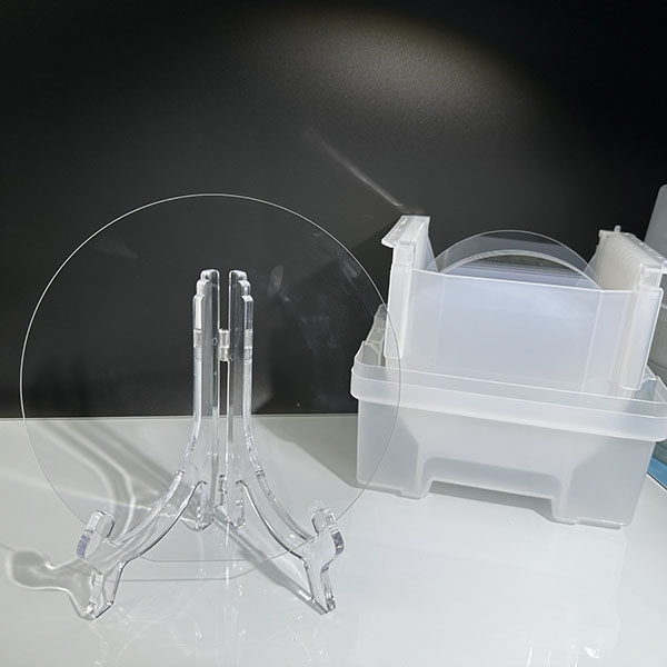
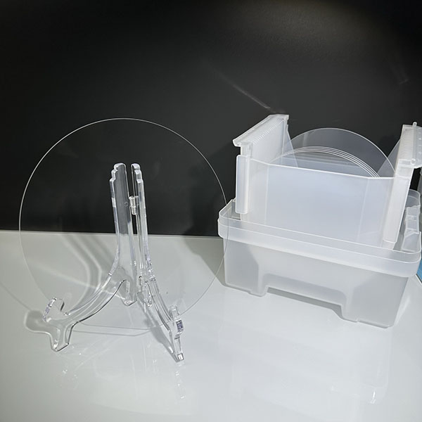
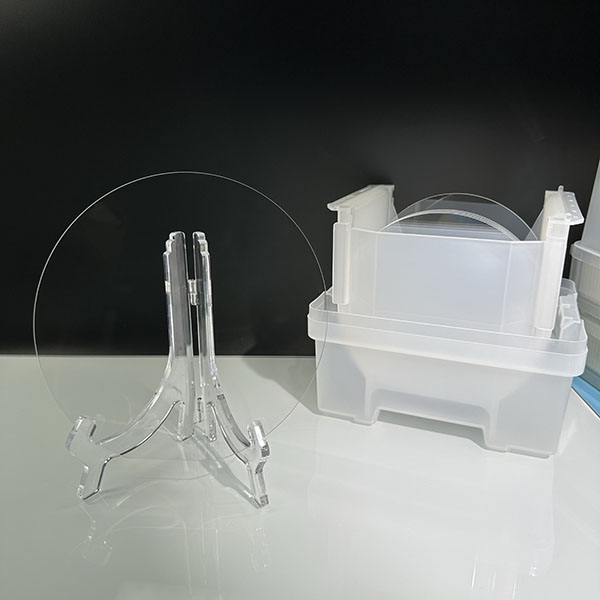
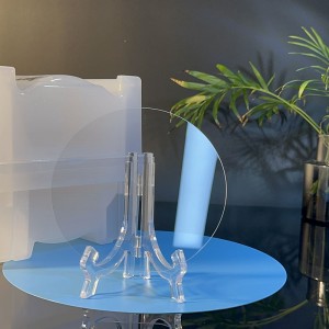
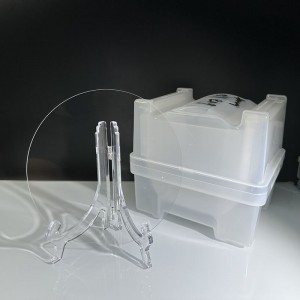
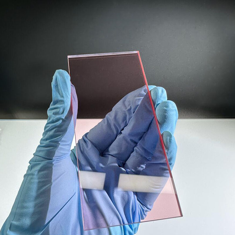
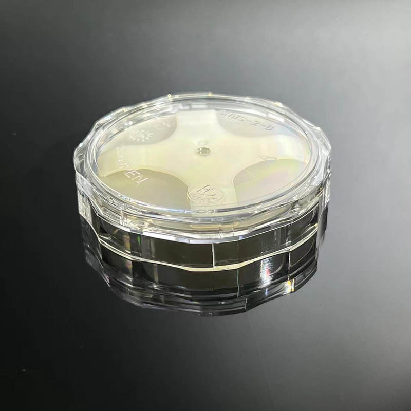
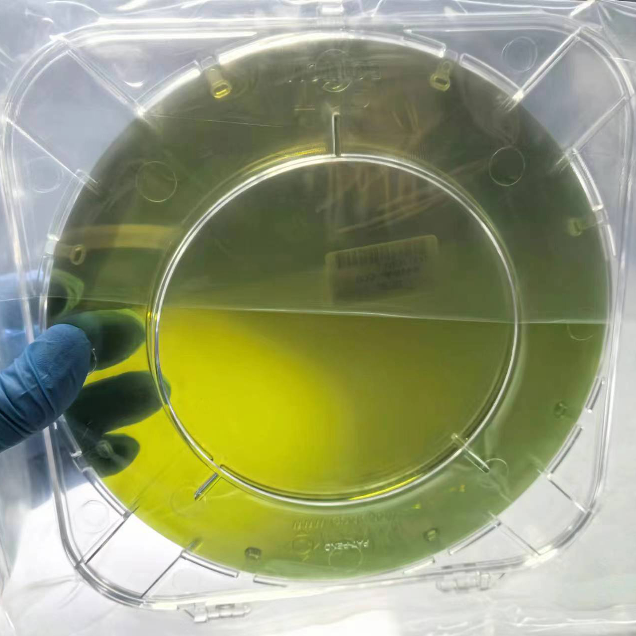
156mm 159mm 6 inch Sapphire Wafer for carrier C-Plane DSP TTV
Specification
| Item | 6-inch C-plane(0001) Sapphire Wafers | |
| Crystal Materials | 99,999%, High Purity, Monocrystalline Al2O3 | |
| Grade | Prime, Epi-Ready | |
| Surface Orientation | C-plane(0001) | |
| C-plane off-angle toward M-axis 0.2 +/- 0.1° | ||
| Diameter | 100.0 mm +/- 0.1 mm | |
| Thickness | 650 μm +/- 25 μm | |
| Primary Flat Orientation | C-plane(00-01) +/- 0.2° | |
| Single Side Polished | Front Surface | Epi-polished, Ra < 0.2 nm (by AFM) |
| (SSP) | Back Surface | Fine ground, Ra = 0.8 μm to 1.2 μm |
| Double Side Polished | Front Surface | Epi-polished, Ra < 0.2 nm (by AFM) |
| (DSP) | Back Surface | Epi-polished, Ra < 0.2 nm (by AFM) |
| TTV | < 20 μm | |
| BOW | < 20 μm | |
| WARP | < 20 μm | |
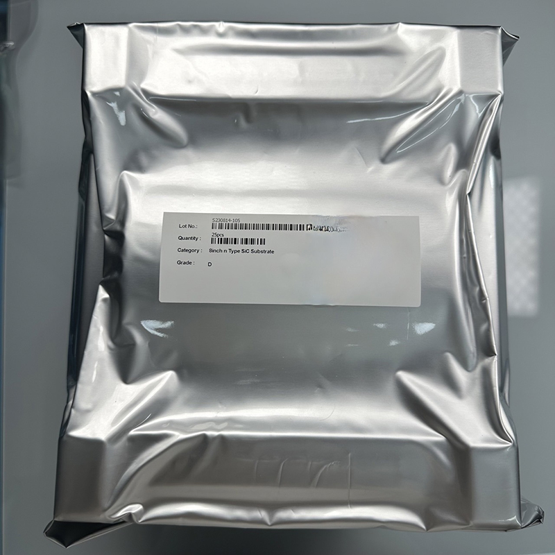
| Cleaning / Packaging | Class 100 cleanroom cleaning and vacuum packaging, | |
| 25 pieces in one cassette packaging or single piece packaging. | ||
The Kylopoulos method (KY method) is currently used by many companies in China to produce sapphire crystals for use in the electronics and optics industries.
In this process, high-purity aluminium oxide is melted in a crucible at temperatures above 2100 degrees Celsius. Usually the crucible is made of tungsten or molybdenum. A precisely oriented seed crystal is immersed in the molten alumina. The seed crystal is slowly pulled upwards and may be rotated simultaneously. By precisely controlling the temperature gradient, the pulling rate and the cooling rate, a large, single-crystal, nearly cylindrical ingot can be produced from the melt.
After the single crystal sapphire ingots are grown, they are drilled into cylindrical rods, which are then cut to the desired window thickness and finally polished to the desired surface finish.
Detailed Diagram
