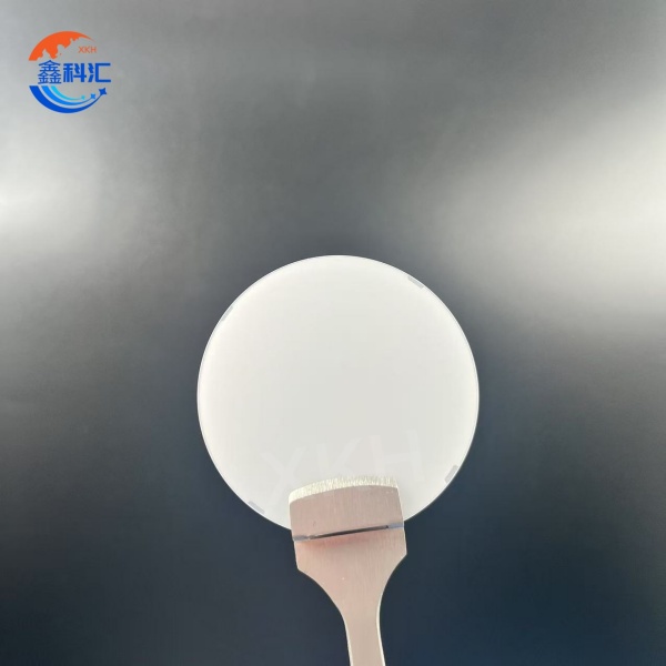
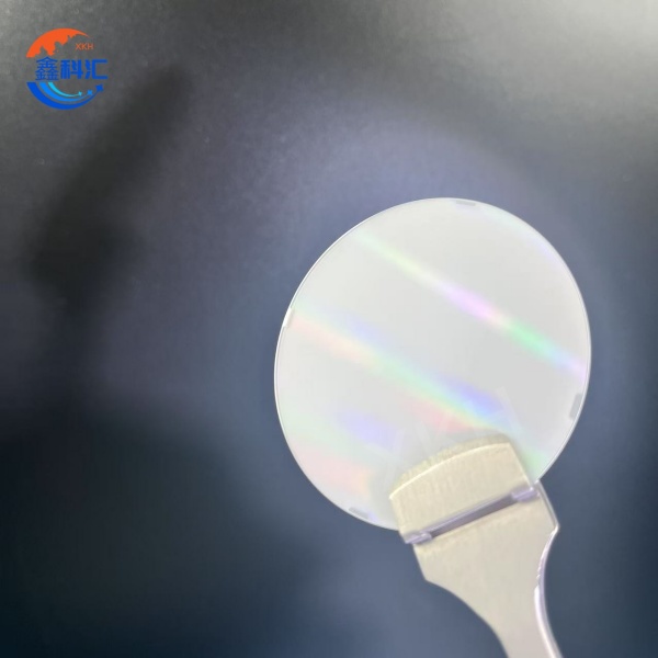
2 inch 4 inch 6 inch Patterned Sapphire Substrate (PSS) on which GaN material is grown can use for LED lighting


Main features
1. Structural characteristics:
The PSS surface has an orderly cone or triangular conical pattern whose shape, size and distribution can be controlled by adjusting the etching process parameters.
These graphic structures help to change the propagation path of light and reduce the total reflection of light, thus improving the efficiency of light extraction.
2. Material characteristics:
PSS uses high-quality sapphire as the substrate material, which has the characteristics of high hardness, high thermal conductivity, good chemical stability and optical transparency.
These characteristics enable PSS to withstand harsh environments such as high temperatures and pressures while maintaining excellent optical performance.
3. Optical performance:
By changing the multiple scattering at the interface between GaN and sapphire substrate, PSS makes the photons that are completely reflected inside GaN layer have a chance to escape from sapphire substrate.
This feature significantly improves the light extraction efficiency of the LED and enhances the luminous intensity of the LED.
4. Process characteristics:
The manufacturing process of PSS is relatively complex, involving multiple steps such as lithography and etching, and requires high-precision equipment and process control.
However, with the continuous advancement of technology and the reduction of costs, the manufacturing process of PSS is gradually optimized and improved.
Core advantage
1.Improve light extraction efficiency: PSS significantly improves the light extraction efficiency of LED by changing the light propagation path and reducing total reflection.
2.Prolong LED life: PSS can reduce the dislocation density of GaN epitaxial materials, thereby reducing the non-radiative recombination and reverse leakage current in the active region, extending the life of LED.
3.Improve LED brightness: Due to the improvement of light extraction efficiency and the extension of LED life, the LED luminous intensity on the PSS is significantly enhanced.
4.Reduce production costs: Although the manufacturing process of PSS is relatively complex, it can significantly improve the luminous efficiency and life of LED, thereby reducing production costs to a certain extent and improving the competitiveness of the product.
Main application areas
1. LED lighting: PSS as a substrate material for LED chips, can significantly improve the luminous efficiency and life of LED.
In the field of LED lighting, PSS is widely used in various lighting products, such as street lamps, table lamps, car lights and so on.
2.Semiconductor devices: In addition to LED lighting, PSS can also be used to manufacture other semiconductor devices, such as light detectors, lasers, etc. These devices have a wide range of applications in communication, medical, military and other fields.
3.Optoelectronic integration: The optical properties and stability of PSS make it one of the ideal materials in the field of optoelectronic integration.In optoelectronic integration, PSS can be used to make optical waveguides, optical switches and other components to realize the transmission and processing of optical signals.
Technical parameters
| Item | Patterned Sapphire Substrate(2~6inch) | ||
| Diameter | 50.8 ± 0.1 mm | 100.0 ± 0.2 mm | 150.0 ± 0.3 mm |
| Thickness | 430 ± 25μm | 650 ± 25μm | 1000 ± 25μm |
| Surface Orientation | C-plane (0001) off-angle toward M-axis (10-10) 0.2 ± 0.1° | ||
| C-plane (0001) off-angle toward A-axis (11-20) 0 ± 0.1° | |||
| Primary Flat Orientation | A-Plane (11-20) ± 1.0° | ||
| Primary Flat Length | 16.0 ± 1.0 mm | 30.0 ± 1.0 mm | 47.5 ± 2.0 mm |
| R-Plane | 9-o'clock | ||
| Front Surface Finish | Patterned | ||
| Back Surface Finish | SSP:Fine-ground,Ra=0.8-1.2um; DSP:Epi-polished,Ra<0.3nm | ||
| Laser Mark | Back side | ||
| TTV | ≤8μm | ≤10μm | ≤20μm |
| BOW | ≤10μm | ≤15μm | ≤25μm |
| WARP | ≤12μm | ≤20μm | ≤30μm |
| Edge Exclusion | ≤2 mm | ||
| Pattern Specification | Shape Structure | Dome, Cone,Pyramid | |
| Pattern Height | 1.6~1.8μm | ||
| Pattern Diameter | 2.75~2.85μm | ||
| Pattern Space | 0.1~0.3μm | ||
XKH focuses on the development, production and sales of patterned sapphire substrate (PSS), and is committed to providing high-quality, high-performance PSS products to customers around the world. XKH has advanced manufacturing technology and professional technical team, which can customize PSS products with different specifications and different pattern structures according to customer needs. At the same time, XKH pays attention to product quality and service quality, and is committed to providing customers with a full range of technical support and solutions. In the field of PSS, XKH has accumulated rich experience and advantages, and looks forward to working together with global partners to jointly promote the innovative development of LED lighting, semiconductor devices and other industries.
Detailed Diagram