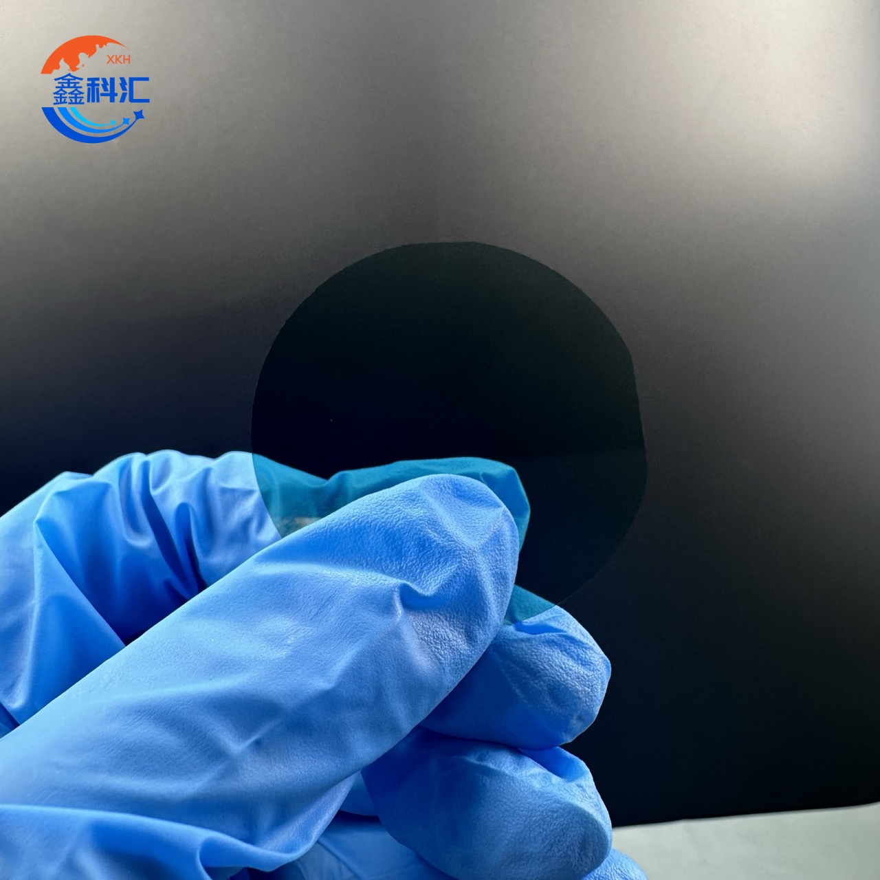
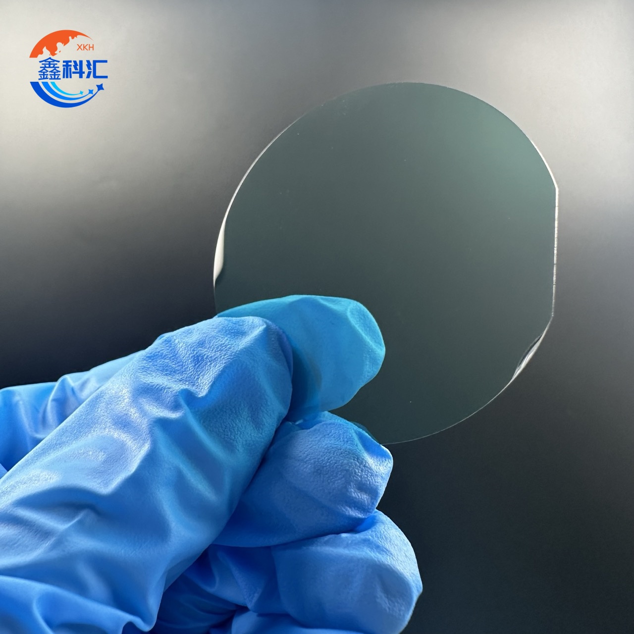
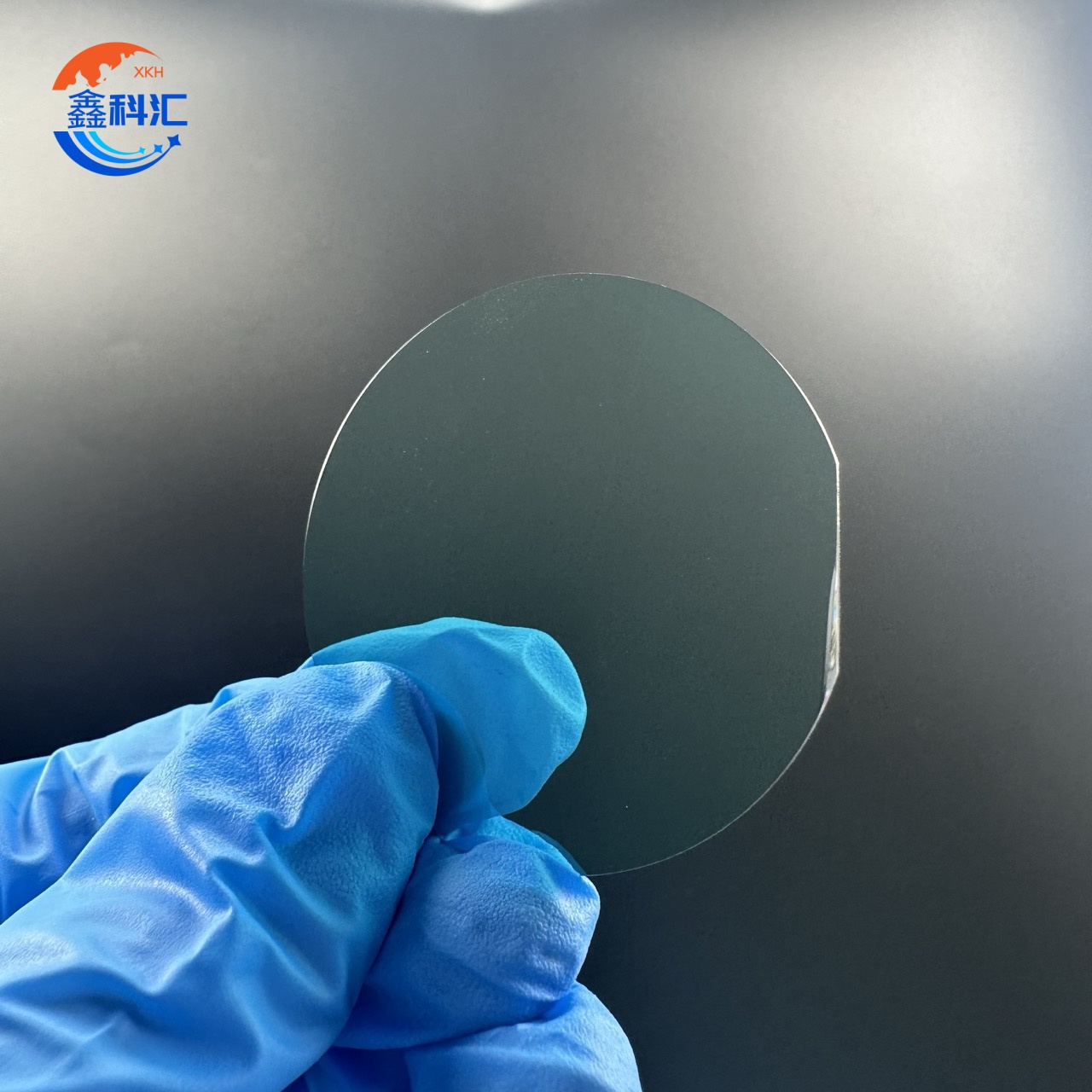
2inch silicon carbide substrate 6H-N double-sided polished diameter 50.8mm production grade research grade
The following are the characteristics of 2inch silicon carbide wafer:
1. Better radiation resistance: SIC wafers have stronger radiation resistance, making them suitable for use in radiation environments. Examples include spacecraft and nuclear facilities.
2. Higher hardness: SIC wafers are harder than silicon, which enhances the durability of wafers during processing.
3. Lower dielectric constant: The dielectric constant of SIC wafers is lower than that of silicon, which helps to reduce parasitic capacitance in the device and improve high-frequency performance.
4. Higher saturated electron drift speed: SIC wafers have a higher saturated electron drift speed than silicon, giving SIC devices an advantage in high-frequency applications.
5. Higher power density: With the above characteristics, SIC wafer devices can achieve higher power output in a smaller size.
2inch silicon carbide wafer has several applications.
1. Power electronics: SiC wafers are widely used in power electronic equipment such as power converters, inverters, and high-voltage switches due to their high breakdown voltage and low power loss characteristics.
2. Electric vehicles: Silicon carbide wafers are used in electric vehicle power electronics to improve efficiency and reduce weight, resulting in faster charging and longer driving range.
3. Renewable energy: Silicon carbide wafers play a vital role in renewable energy applications such as solar inverters and wind power systems, improving energy conversion efficiency and reliability.
4.Aerospace and Defense: SiC wafers are essential in the aerospace and defense industry for high temperature, high power and radiation resistant applications, including aircraft power systems and radar systems.
ZMSH provides product customization services for our silicon carbide wafers. Our wafers are made from high-quality silicon carbide layers sourced from China to ensure durability and reliability. Customers can choose from our selection of wafer sizes and specifications to meet their specific needs.
Our Silicon Carbide wafers come in different models and sizes, the model is Silicon Carbide.
We offer a range of surface treatments including single/double sided polishing with surface roughness ≤1.2nm and flatness Lambda/10. We also offer high/low resistivity options that can be customized to your requirements. Our EPD of ≤1E10/cm2 ensures that our wafers meet the highest industry standards.
We concerns each details of the package , cleaning, anti-static , shock treatment .According to the quantity and shape of the product , we will take a different packaging process! Almost by single wafer cassettes or 25pcs cassette in 100 grade cleaning room.
Detailed Diagram


