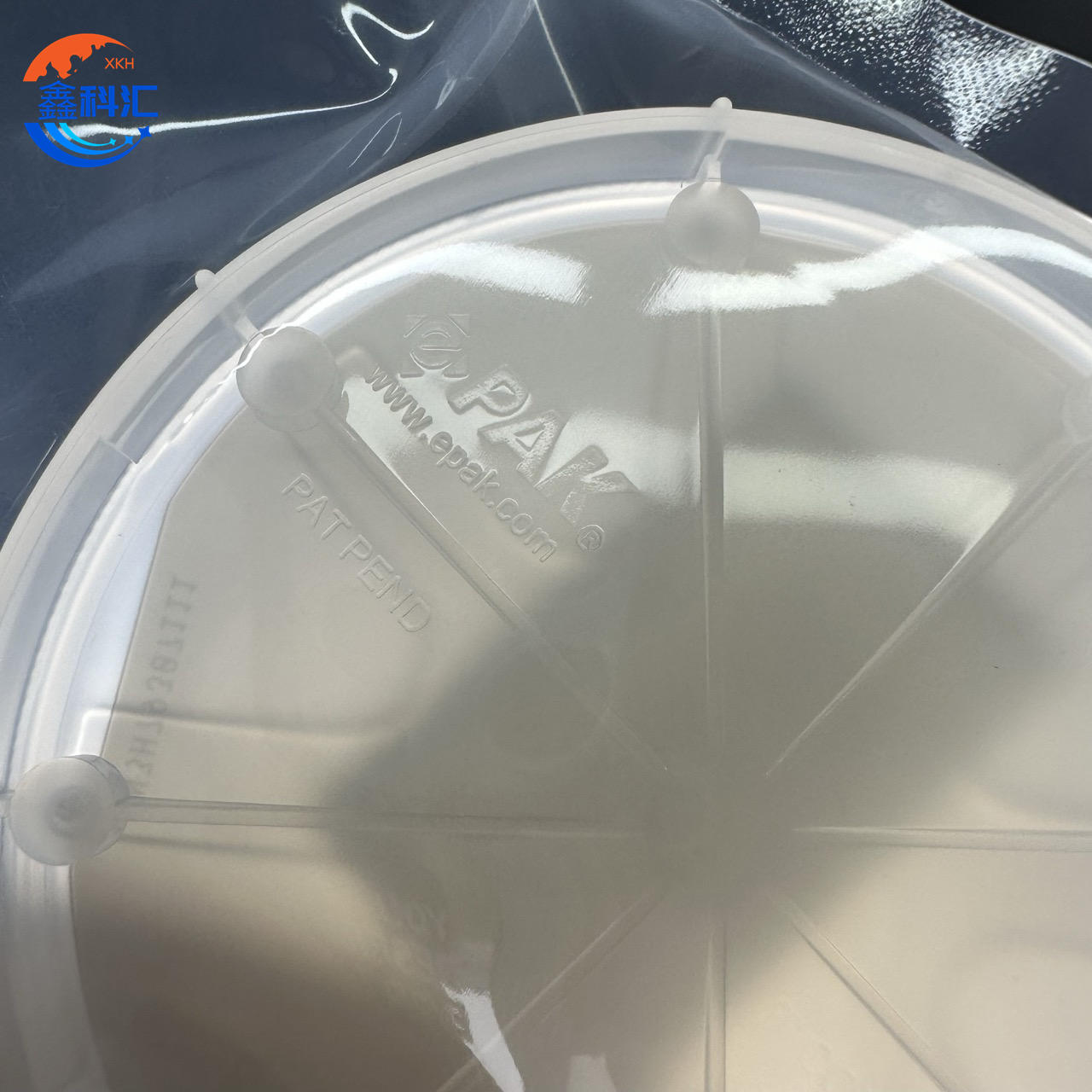
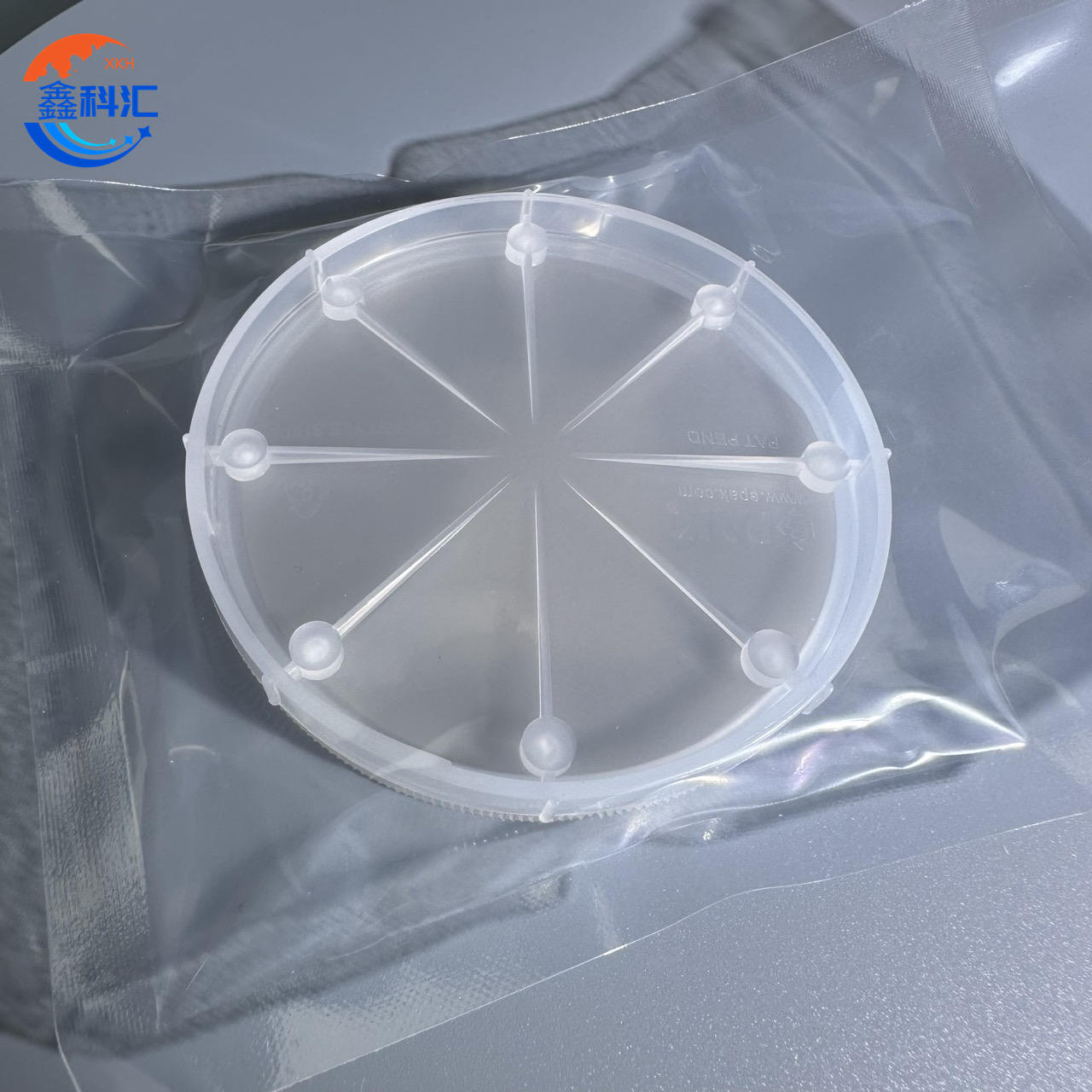
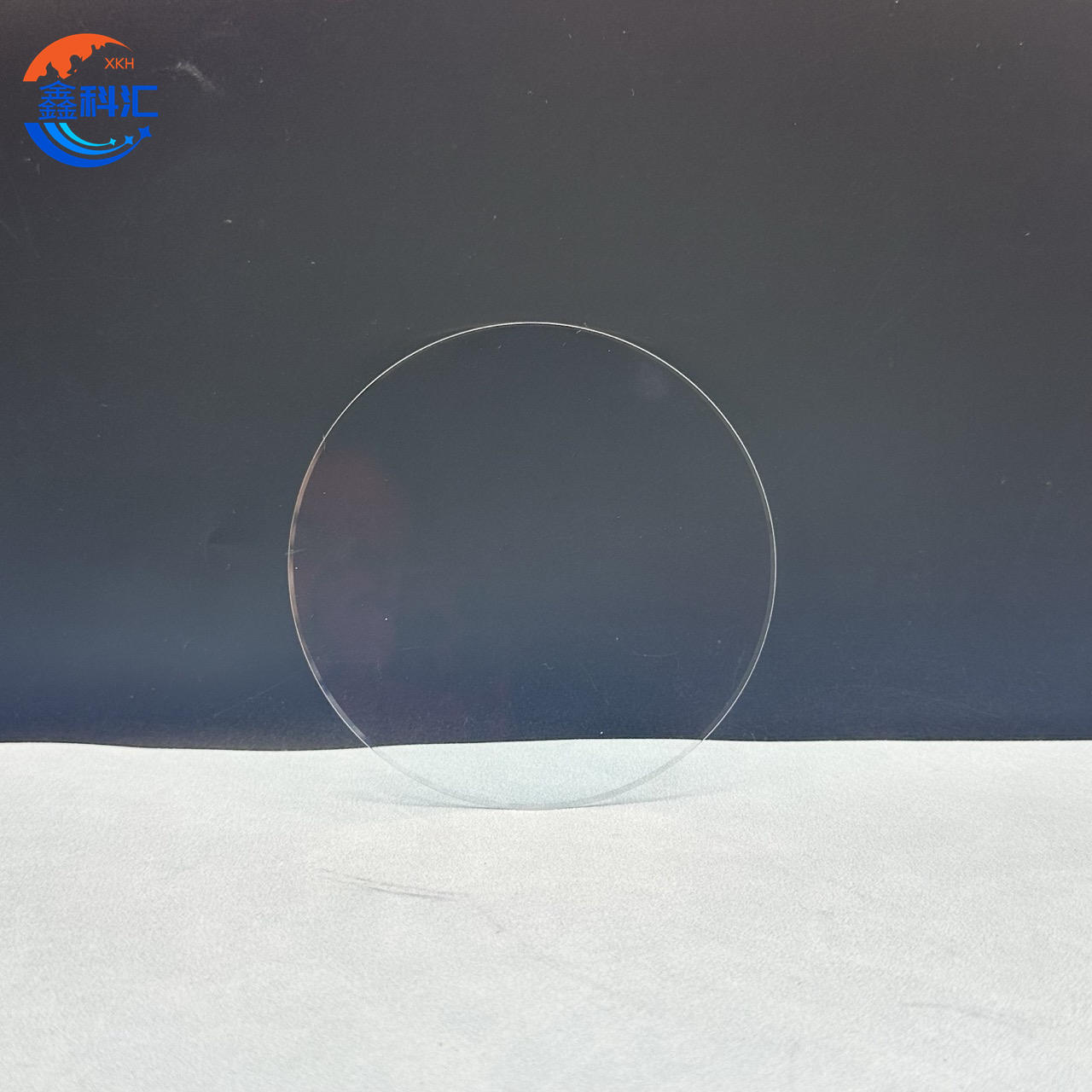
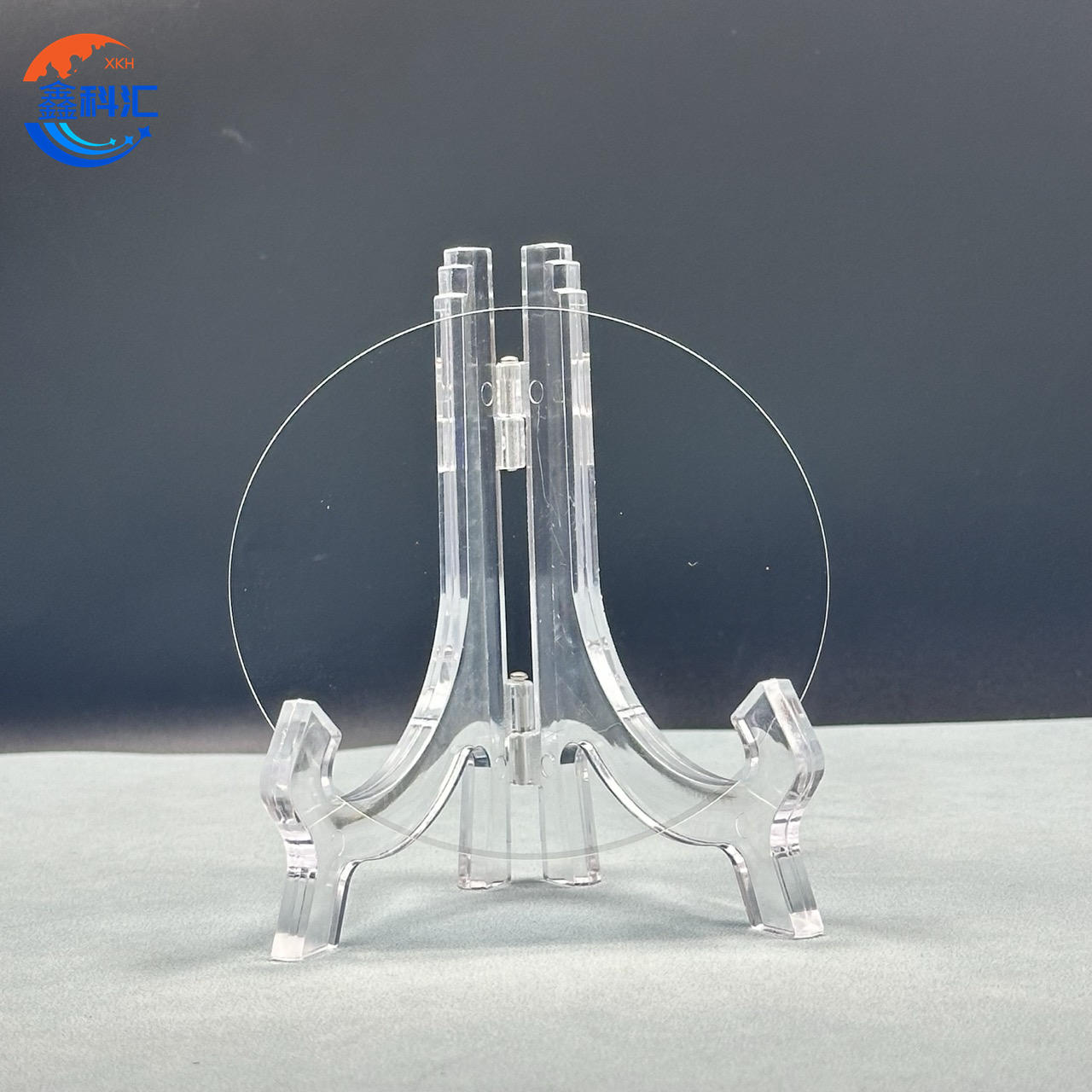
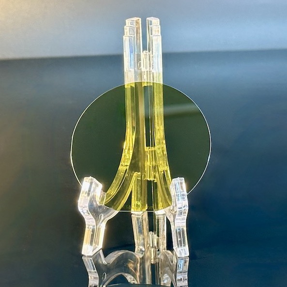
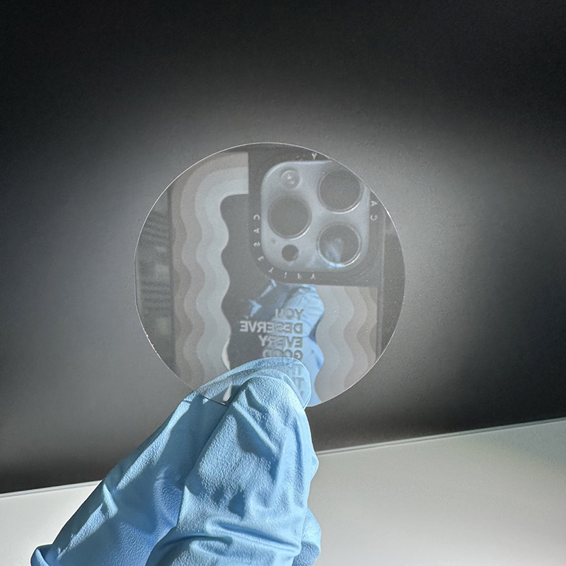
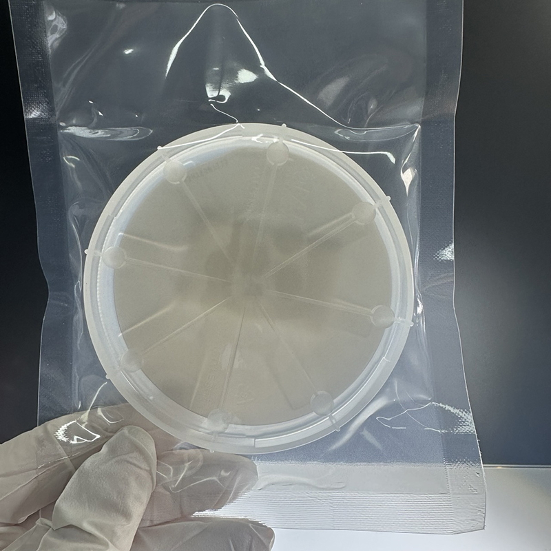
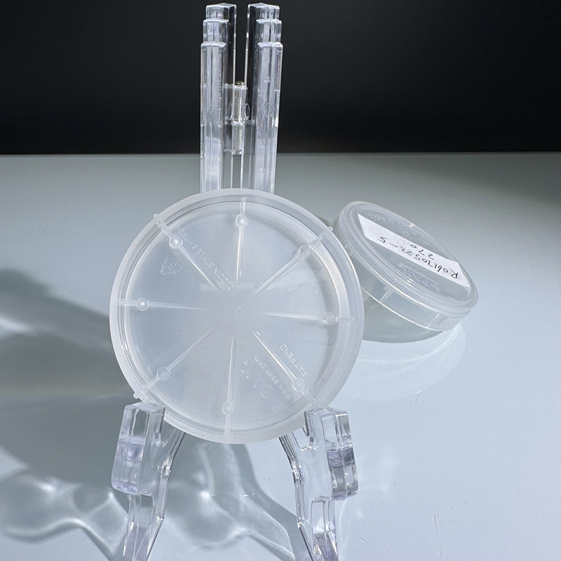
3 inch High Purity (Undoped) Silicon Carbide Wafers semi-Insulating Sic Substrates (HPSl)
Properties
1. Physical and Structural Properties
●Material Type: High Purity (Undoped) Silicon Carbide (SiC)
●Diameter: 3 inches (76.2 mm)
●Thickness: 0.33-0.5 mm, customizable based on application requirements.
●Crystal Structure: 4H-SiC polytype with a hexagonal lattice, known for high electron mobility and thermal stability.
●Orientation:
oStandard: [0001] (C-plane), suitable for a wide range of applications.
oOptional: Off-axis (4° or 8° tilt) for enhanced epitaxial growth of device layers.
●Flatness: Total thickness variation (TTV) ●Surface Quality:
oPolished to oLow-defect density (<10/cm² micropipe density). 2. Electrical Properties ●Resistivity: >109^99 Ω·cm, maintained by the elimination of intentional dopants.
●Dielectric Strength: High voltage endurance with minimal dielectric losses, ideal for high-power applications.
●Thermal Conductivity: 3.5-4.9 W/cm·K, enabling effective heat dissipation in high-performance devices.
3. Thermal and Mechanical Properties
●Wide Bandgap: 3.26 eV, supporting operation under high voltage, high temperature, and high radiation conditions.
●Hardness: Mohs scale 9, ensuring robustness against mechanical wear during processing.
●Thermal Expansion Coefficient: 4.2×10⁻⁶/K4.2 \times 10^{-6}/\text{K}4.2×10−6/K, ensuring dimensional stability under temperature variations.
|
Parameter |
Production Grade |
Research Grade |
Dummy Grade |
Unit |
| Grade | Production Grade | Research Grade | Dummy Grade | |
| Diameter | 76.2 ± 0.5 | 76.2 ± 0.5 | 76.2 ± 0.5 | mm |
| Thickness | 500 ± 25 | 500 ± 25 | 500 ± 25 | µm |
| Wafer Orientation | On-axis: <0001> ± 0.5° | On-axis: <0001> ± 2.0° | On-axis: <0001> ± 2.0° | degree |
| Micropipe Density (MPD) | ≤ 1 | ≤ 5 | ≤ 10 | cm−2^-2−2 |
| Electrical Resistivity | ≥ 1E10 | ≥ 1E5 | ≥ 1E5 | Ω·cm |
| Dopant | Undoped | Undoped | Undoped | |
| Primary Flat Orientation | {1-100} ± 5.0° | {1-100} ± 5.0° | {1-100} ± 5.0° | degree |
| Primary Flat Length | 32.5 ± 3.0 | 32.5 ± 3.0 | 32.5 ± 3.0 | mm |
| Secondary Flat Length | 18.0 ± 2.0 | 18.0 ± 2.0 | 18.0 ± 2.0 | mm |
| Secondary Flat Orientation | 90° CW from primary flat ± 5.0° | 90° CW from primary flat ± 5.0° | 90° CW from primary flat ± 5.0° | degree |
| Edge Exclusion | 3 | 3 | 3 | mm |
| LTV/TTV/Bow/Warp | 3 / 10 / ±30 / 40 | 3 / 10 / ±30 / 40 | 5 / 15 / ±40 / 45 | µm |
| Surface Roughness | Si-face: CMP, C-face: Polished | Si-face: CMP, C-face: Polished | Si-face: CMP, C-face: Polished | |
| Cracks (High-Intensity Light) | None | None | None | |
| Hex Plates (High-Intensity Light) | None | None | Cumulative area 10% | % |
| Polytype Areas (High-Intensity Light) | Cumulative area 5% | Cumulative area 20% | Cumulative area 30% | % |
| Scratches (High-Intensity Light) | ≤ 5 scratches, cumulative length ≤ 150 | ≤ 10 scratches, cumulative length ≤ 200 | ≤ 10 scratches, cumulative length ≤ 200 | mm |
| Edge Chipping | None ≥ 0.5 mm width/depth | 2 allowed ≤ 1 mm width/depth | 5 allowed ≤ 5 mm width/depth | mm |
| Surface Contamination | None | None | None |
Applications
1. Power Electronics
The wide bandgap and high thermal conductivity of HPSI SiC substrates make them ideal for power devices operating in extreme conditions, such as:
●High-Voltage Devices: Including MOSFETs, IGBTs, and Schottky Barrier Diodes (SBDs) for efficient power conversion.
●Renewable Energy Systems: Such as solar inverters and wind turbine controllers.
●Electric Vehicles (EVs): Used in inverters, chargers, and powertrain systems to improve efficiency and reduce size.
2. RF and Microwave Applications
The high resistivity and low dielectric losses of HPSI wafers are essential for radio-frequency (RF) and microwave systems, including:
●Telecommunication Infrastructure: Base stations for 5G networks and satellite communications.
●Aerospace and Defense: Radar systems, phased-array antennas, and avionics components.
3. Optoelectronics
The transparency and wide bandgap of 4H-SiC enable its use in optoelectronic devices, such as:
●UV Photodetectors: For environmental monitoring and medical diagnostics.
●High-Power LEDs: Supporting solid-state lighting systems.
●Laser Diodes: For industrial and medical applications.
4. Research and Development
HPSI SiC substrates are widely used in academic and industrial R&D labs for exploring advanced material properties and device fabrication, including:
●Epitaxial Layer Growth: Studies on defect reduction and layer optimization.
●Carrier Mobility Studies: Investigation of electron and hole transport in high-purity materials.
●Prototyping: Initial development of novel devices and circuits.
Advantages
Superior Quality:
High purity and low defect density provide a reliable platform for advanced applications.
Thermal Stability:
Excellent heat dissipation properties allow devices to operate efficiently under high power and temperature conditions.
Broad Compatibility:
Available orientations and custom thickness options ensure adaptability for various device requirements.
Durability:
Exceptional hardness and structural stability minimize wear and deformation during processing and operation.
Versatility:
Suitable for a wide range of industries, from renewable energy to aerospace and telecommunications.
Conclusion
The 3-inch High Purity Semi-Insulating Silicon Carbide wafer represents the pinnacle of substrate technology for high-power, high-frequency, and optoelectronic devices. Its combination of excellent thermal, electrical, and mechanical properties ensures reliable performance in challenging environments. From power electronics and RF systems to optoelectronics and advanced R&D, these HPSI substrates provide the foundation for tomorrow’s innovations.
For more information or to place an order, please contact us. Our technical team is available to provide guidance and customization options tailored to your needs.
Detailed Diagram
