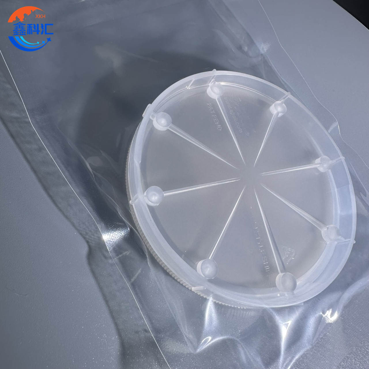
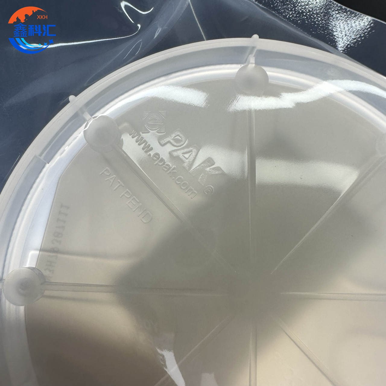
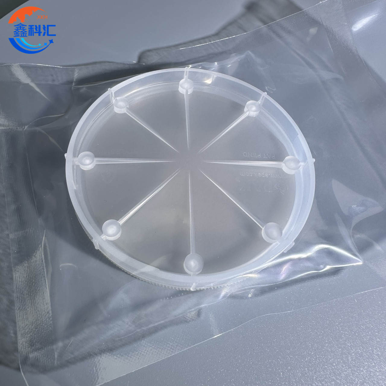
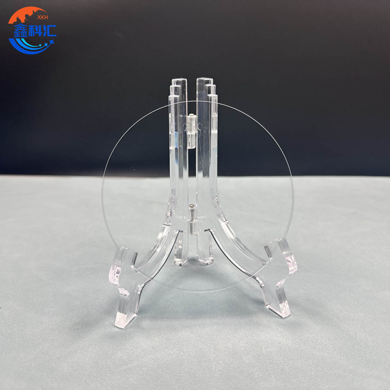
3inch High purity Semi-Insulating (HPSI)SiC wafer 350um Dummy grade Prime grade
Application
HPSI SiC wafers are pivotal in enabling next-generation power devices, which are used in a variety of high-performance applications:
Power Conversion Systems: SiC wafers serve as the core material for power devices such as power MOSFETs, diodes, and IGBTs, which are crucial for efficient power conversion in electrical circuits. These components are found in high-efficiency power supplies, motor drives, and industrial inverters.
Electric Vehicles (EVs): The growing demand for electric vehicles necessitates the use of more efficient power electronics, and SiC wafers are at the forefront of this transformation. In EV powertrains, these wafers provide high efficiency and fast switching capabilities, which contribute to faster charging times, longer range, and enhanced overall vehicle performance.
Renewable Energy: In renewable energy systems such as solar and wind power, SiC wafers are used in inverters and converters that enable more efficient energy capture and distribution. The high thermal conductivity and superior breakdown voltage of SiC ensure that these systems operate reliably, even under extreme environmental conditions.
Industrial Automation and Robotics: High-performance power electronics in industrial automation systems and robotics require devices capable of switching quickly, handling large power loads, and operating under high stress. SiC-based semiconductors meet these requirements by providing higher efficiency and robustness, even in harsh operating environments.
Telecommunication Systems: In telecommunications infrastructure, where high reliability and efficient energy conversion are critical, SiC wafers are used in power supplies and DC-DC converters. SiC devices help reduce energy consumption and enhance system performance in data centers and communication networks.
By providing a robust foundation for high-power applications, the HPSI SiC wafer enables the development of energy-efficient devices, helping industries transition to greener, more sustainable solutions.
Properties
|
operty |
Production Grade |
Research Grade |
Dummy Grade |
| Diameter | 75.0 mm ± 0.5 mm | 75.0 mm ± 0.5 mm | 75.0 mm ± 0.5 mm |
| Thickness | 350 µm ± 25 µm | 350 µm ± 25 µm | 350 µm ± 25 µm |
| Wafer Orientation | On axis: <0001> ± 0.5° | On axis: <0001> ± 2.0° | On axis: <0001> ± 2.0° |
| Micropipe Density for 95% of Wafers (MPD) | ≤ 1 cm⁻² | ≤ 5 cm⁻² | ≤ 15 cm⁻² |
| Electrical Resistivity | ≥ 1E7 Ω·cm | ≥ 1E6 Ω·cm | ≥ 1E5 Ω·cm |
| Dopant | Undoped | Undoped | Undoped |
| Primary Flat Orientation | {11-20} ± 5.0° | {11-20} ± 5.0° | {11-20} ± 5.0° |
| Primary Flat Length | 32.5 mm ± 3.0 mm | 32.5 mm ± 3.0 mm | 32.5 mm ± 3.0 mm |
| Secondary Flat Length | 18.0 mm ± 2.0 mm | 18.0 mm ± 2.0 mm | 18.0 mm ± 2.0 mm |
| Secondary Flat Orientation | Si face up: 90° CW from primary flat ± 5.0° | Si face up: 90° CW from primary flat ± 5.0° | Si face up: 90° CW from primary flat ± 5.0° |
| Edge Exclusion | 3 mm | 3 mm | 3 mm |
| LTV/TTV/Bow/Warp | 3 µm / 10 µm / ±30 µm / 40 µm | 3 µm / 10 µm / ±30 µm / 40 µm | 5 µm / 15 µm / ±40 µm / 45 µm |
| Surface Roughness | C-face: Polished, Si-face: CMP | C-face: Polished, Si-face: CMP | C-face: Polished, Si-face: CMP |
| Cracks (inspected by high intensity light) | None | None | None |
| Hex Plates (inspected by high intensity light) | None | None | Cumulative area 10% |
| Polytype Areas (inspected by high intensity light) | Cumulative area 5% | Cumulative area 5% | Cumulative area 10% |
| Scratches (inspected by high intensity light) | ≤ 5 scratches, cumulative length ≤ 150 mm | ≤ 10 scratches, cumulative length ≤ 200 mm | ≤ 10 scratches, cumulative length ≤ 200 mm |
| Edge Chipping | None permitted ≥ 0.5 mm width and depth | 2 allowed, ≤ 1 mm width and depth | 5 allowed, ≤ 5 mm width and depth |
| Surface Contamination (inspected by high intensity light) | None | None | None |
Key Advantages
Superior Thermal Performance: SiC’s high thermal conductivity ensures efficient heat dissipation in power devices, allowing them to operate at higher power levels and frequencies without overheating. This translates to smaller, more efficient systems and longer operational lifespans.
High Breakdown Voltage: With a wider bandgap compared to silicon, SiC wafers support high-voltage applications, making them ideal for power electronic components that need to withstand high breakdown voltages, such as in electric vehicles, grid power systems, and renewable energy systems.
Reduced Power Loss: The low on-resistance and fast switching speeds of SiC devices result in reduced energy loss during operation. This not only improves efficiency but also enhances the overall energy savings of systems in which they are deployed.
Enhanced Reliability in Harsh Environments: SiC’s robust material properties allow it to perform in extreme conditions, such as high temperatures (up to 600°C), high voltages, and high frequencies. This makes SiC wafers suitable for demanding industrial, automotive, and energy applications.
Energy Efficiency: SiC devices offer a higher power density than traditional silicon-based devices, reducing the size and weight of power electronic systems while improving their overall efficiency. This leads to cost savings and a smaller environmental footprint in applications such as renewable energy and electric vehicles.
Scalability: The 3-inch diameter and precise manufacturing tolerances of the HPSI SiC wafer ensure that it is scalable for mass production, meeting both research and commercial manufacturing requirements.
Conclusion
The HPSI SiC wafer, with its 3-inch diameter and 350 µm ± 25 µm thickness, is the optimal material for the next generation of high-performance power electronic devices. Its unique combination of thermal conductivity, high breakdown voltage, low energy loss, and reliability under extreme conditions makes it an essential component for various applications in power conversion, renewable energy, electric vehicles, industrial systems, and telecommunications.
This SiC wafer is particularly suited for industries seeking to achieve higher efficiency, greater energy savings, and improved system reliability. As power electronics technology continues to evolve, the HPSI SiC wafer provides the foundation for the development of next-generation, energy-efficient solutions, driving the transition to a more sustainable, low-carbon future.
Detailed Diagram


