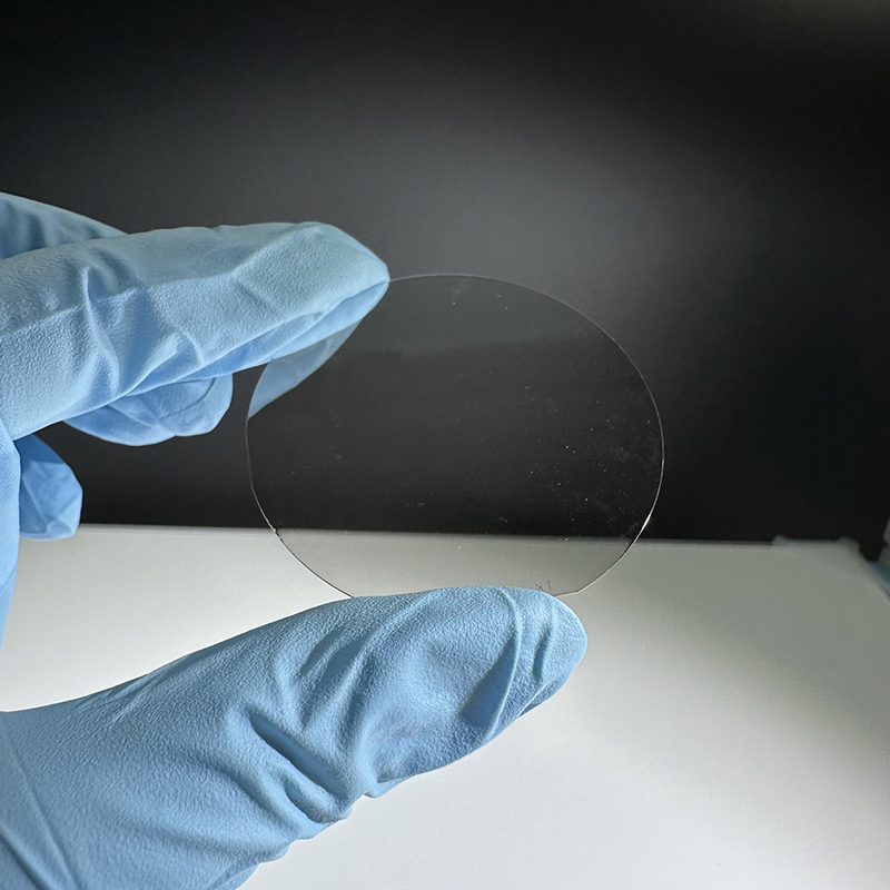
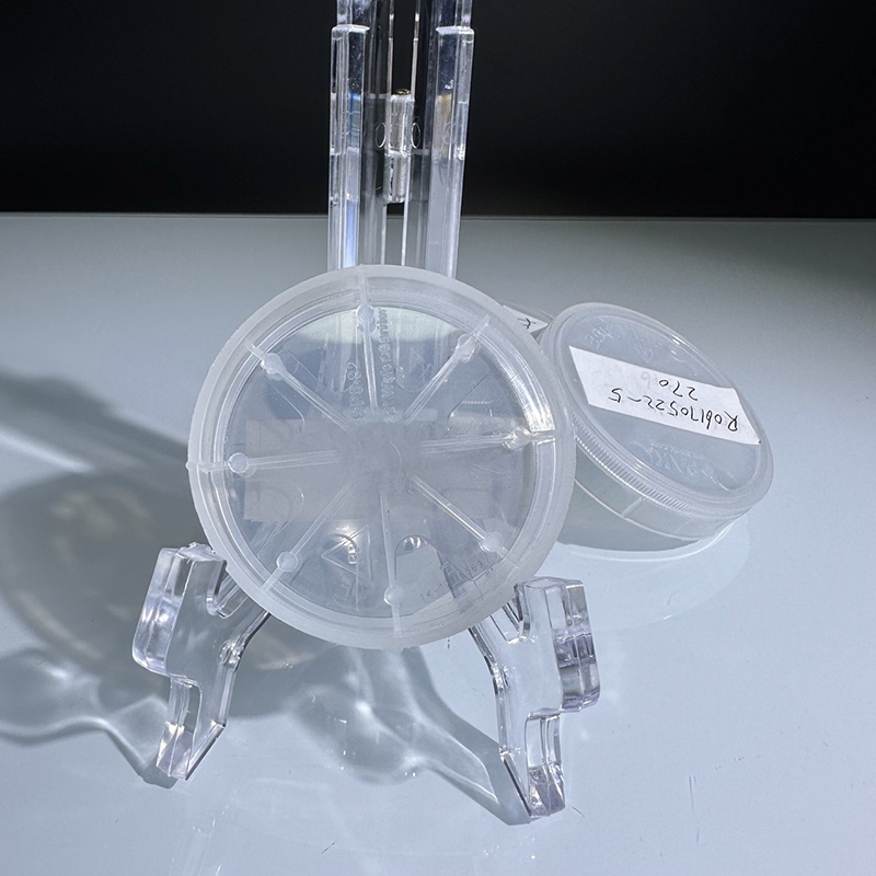
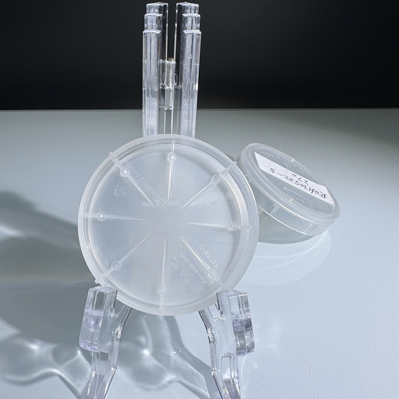
4H-semi HPSI 2inch SiC substrate wafer Production Dummy Research grade
Semi-insulating silicon carbide substrate SiC wafers
Silicon carbide substrate is mainly divided into conductive and semi-insulating type, conductive silicon carbide substrate to n-type substrate is mainly used for epitaxial GaN-based LED and other optoelectronic devices, SiC-based power electronic devices, etc., and semi-insulating SiC silicon carbide substrate is mainly used for epitaxial manufacture of GaN high-power radio frequency devices. In addition high-purity semi-insulation HPSI and SI semi-insulation is different, high-purity semi-insulation carrier concentration of 3.5 * 1013 ~ 8 * 1015/cm3 range, with high electron mobility; semi-insulation is a high-resistance materials, resistivity is very high, generally used for microwave device substrates, non-conductive.
Semi-insulating Silicon Carbide substrate sheet SiC wafer
SiC crystal structure determines its physical, relative to Si and GaAs, SiC has for the physical properties; forbidden band width is large, close to 3 times that of Si, to ensure that the device works at high temperatures under the long-term reliability; breakdown field strength is high, is 1O times that of Si, to ensure that the device voltage capacity, improve the device voltage value; saturation electron rate is large, is 2 times that of Si, to increase the device's frequency and power density; thermal conductivity is high, more than Si, the thermal conductivity is high, the thermal conductivity is high, the thermal conductivity is high, the thermal conductivity is high, more than the Si, the thermal conductivity is high, the thermal conductivity is high. High thermal conductivity, more than 3 times that of Si, increasing the heat dissipation capacity of the device and realising the miniaturisation of the device.
Detailed Diagram


