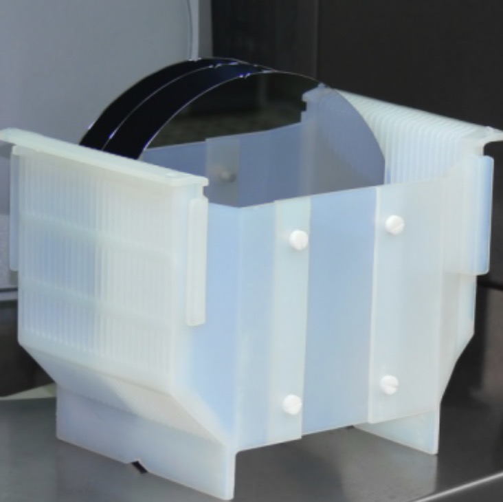
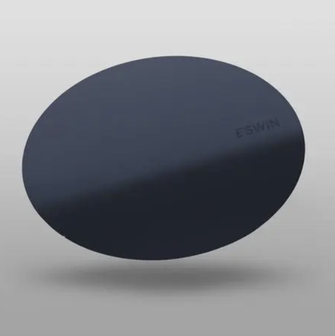
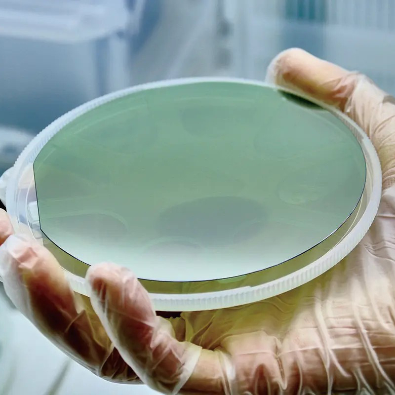
4inch SiC Epi wafer for MOS or SBD
Epitaxy refers to the growth of a layer of higher quality single crystal material on the surface of a silicon carbide substrate. Among them, the growth of gallium nitride epitaxial layer on a semi-insulating silicon carbide substrate is called heterogeneous epitaxy; the growth of a silicon carbide epitaxial layer on the surface of a conductive silicon carbide substrate is called homogeneous epitaxy.
Epitaxial is in accordance with the device design requirements of the growth of the main functional layer, largely determines the performance of the chip and the device, the cost of 23%. The main methods of SiC thin film epitaxy at this stage include: chemical vapor deposition (CVD), molecular beam epitaxy (MBE), liquid phase epitaxy (LPE), and pulsed laser deposition and sublimation (PLD).
Epitaxy is a very critical link in the whole industry. By growing GaN epitaxial layers on semi-insulating silicon carbide substrates, GaN epitaxial wafers based on silicon carbide are produced, which can be further made into GaN RF devices such as high electron mobility transistors (HEMTs);
By growing silicon carbide epitaxial layer on conductive substrate to get silicon carbide epitaxial wafer, and in the epitaxial layer on the manufacture of Schottky diodes, gold-oxygen half-field effect transistors, insulated gate bipolar transistors and other power devices, so the quality of the epitaxial on the performance of the device is very big impact on the development of the industry is also playing a very critical role.
Detailed Diagram


