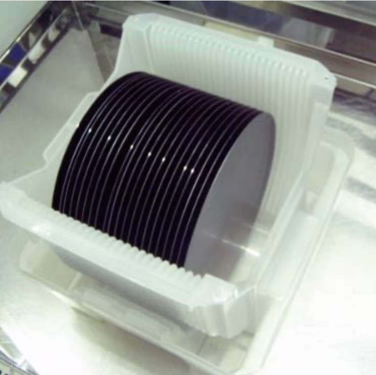
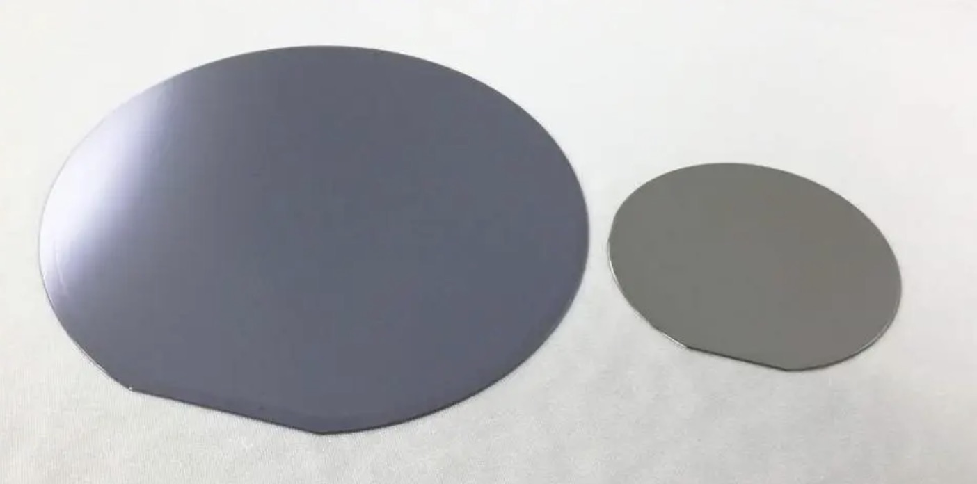
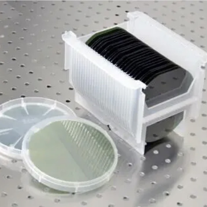
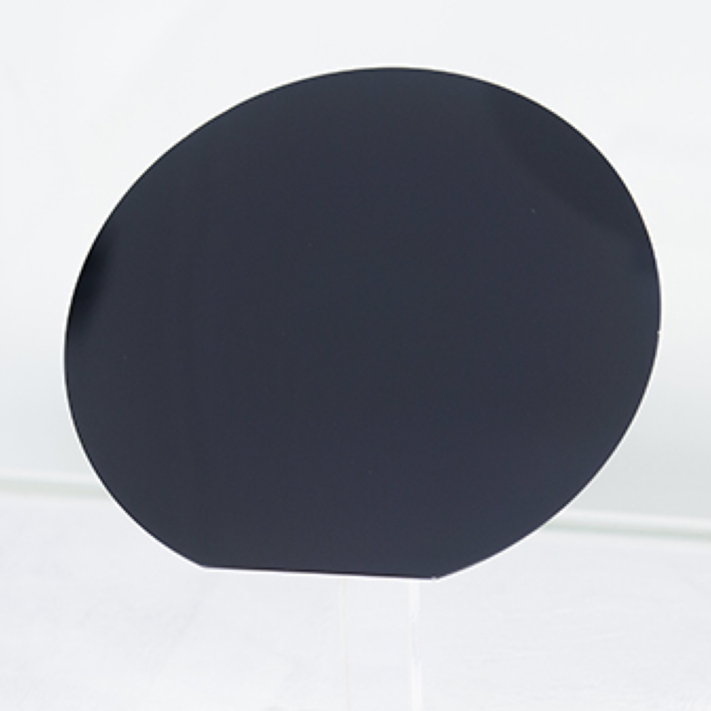
6inch SiC Epitaxiy wafer N/P type accept customized
The preparation process of silicon carbide epitaxial wafer is a method using Chemical Vapor Deposition (CVD) technology. The following are the relevant technical principles and preparation process steps:
Technical principle:
Chemical Vapor Deposition: Utilizing the raw material gas in the gas phase, under specific reaction conditions, it is decomposed and deposited on the substrate to form the desired thin film.
Gas-phase reaction: Through pyrolysis or cracking reaction, various raw material gases in the gas phase are chemically changed in the reaction chamber.
Preparation process steps:
Substrate treatment: The substrate is subjected to surface cleaning and pretreatment to ensure the quality and crystallinity of the epitaxial wafer.
Reaction chamber debugging: adjust the temperature, pressure and flow rate of the reaction chamber and other parameters to ensure the stability and control of the reaction conditions.
Raw material supply: supply the required gas raw materials into the reaction chamber, mixing and controlling the flow rate as needed.
Reaction process: By heating the reaction chamber, the gaseous feedstock undergoes a chemical reaction in the chamber to produce the desired deposit, i.e. silicon carbide film.
Cooling and unloading: At the end of the reaction, the temperature is gradually lowered to cool and solidify the deposits in the reaction chamber.
Epitaxial wafer annealing and post-processing: the deposited epitaxial wafer is annealed and post-processed to improve its electrical and optical properties.
The specific steps and conditions of the silicon carbide epitaxial wafer preparation process may vary depending on the specific equipment and requirements. The above is only a general process flow and principle, the specific operation needs to be adjusted and optimized according to the actual situation.
Detailed Diagram


