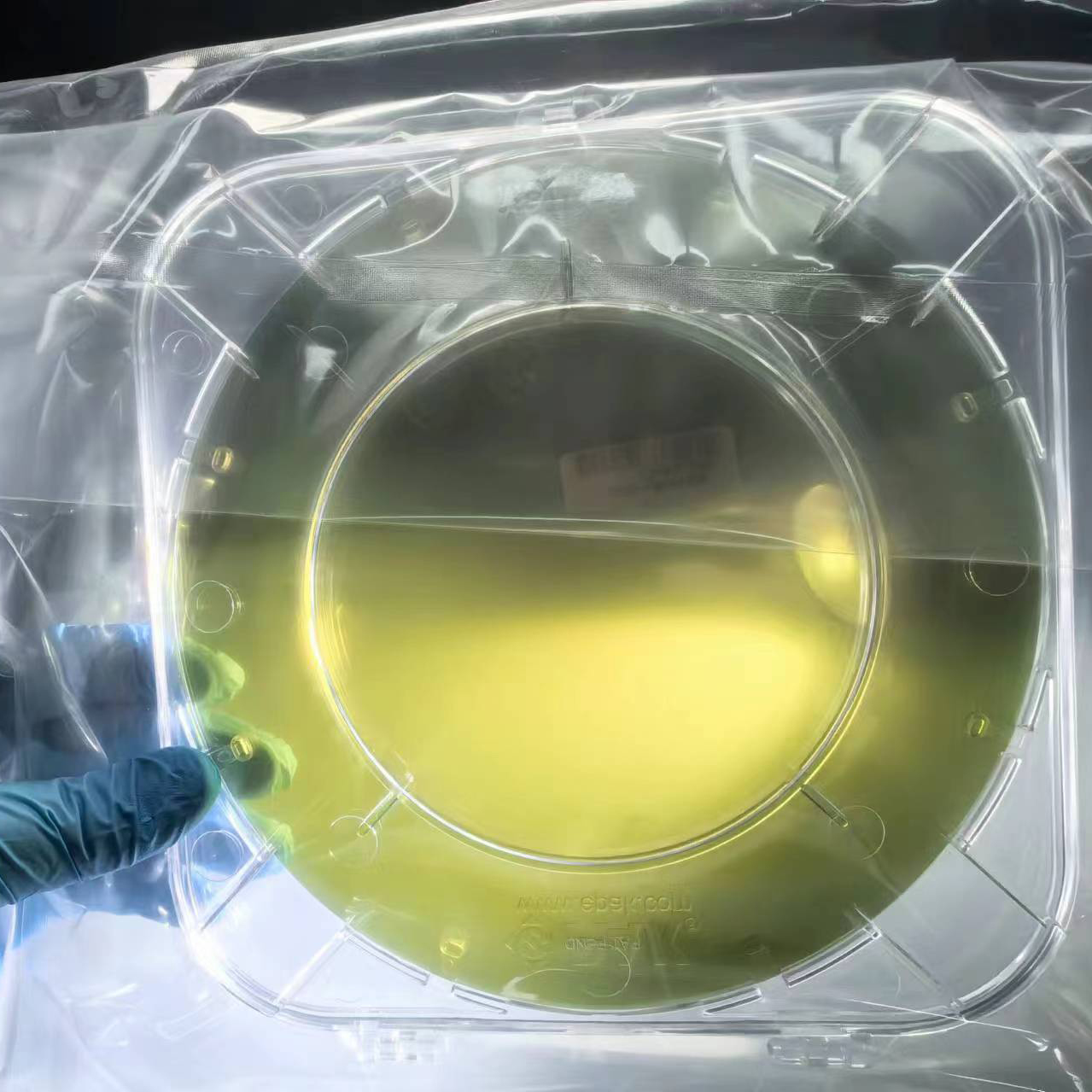
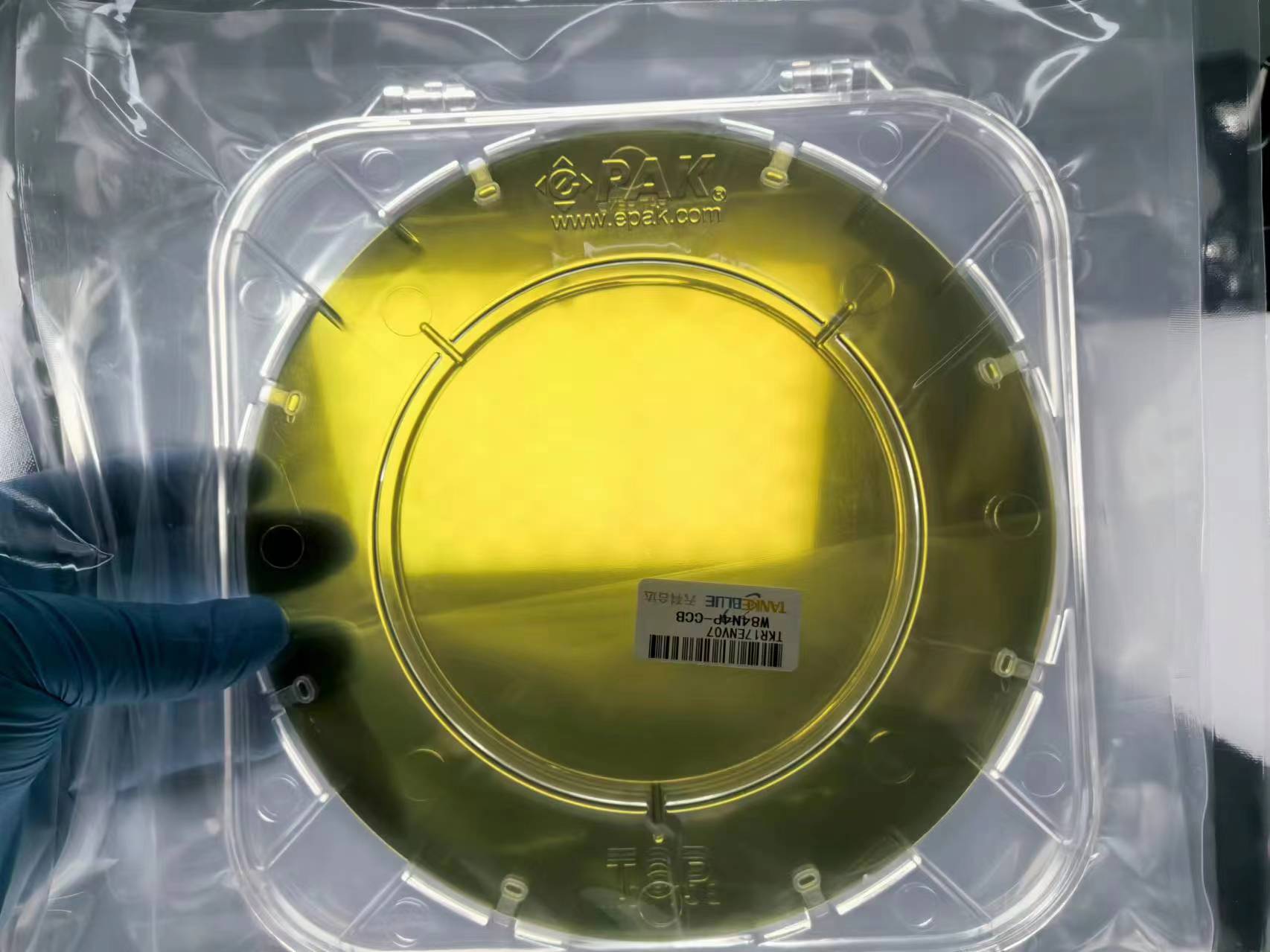
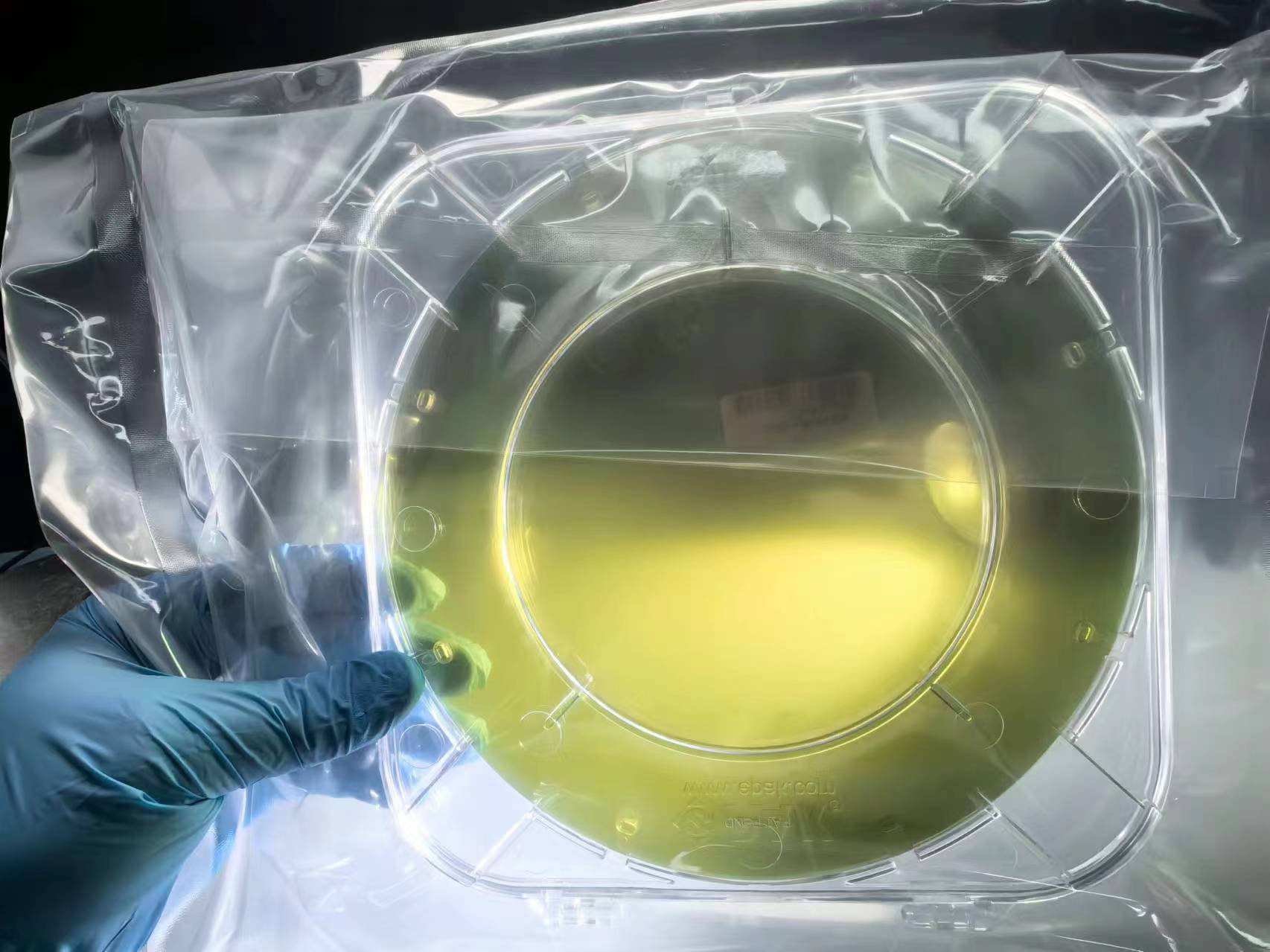
8inch SiC Production grade wafer 4H-N SiC substrate


The following table shows the specifications of our 8inch SiC wafers:
|
8inch N-type SiC DSP Specs |
|||||
| Number | Item | Unit | Production | Research | Dummy |
| 1:parameters | |||||
| 1.1 | polytype | -- | 4H | 4H | 4H |
| 1.2 | surface orientation | ° | <11-20>4±0.5 | <11-20>4±0.5 | <11-20>4±0.5 |
| 2:Electrical parameter | |||||
| 2.1 | dopant | -- | n-type Nitrogen | n-type Nitrogen | n-type Nitrogen |
| 2.2 | resistivity | ohm ·cm | 0.015~0.025 | 0.01~0.03 | NA |
| 3:Mechanical parameter | |||||
| 3.1 | diameter | mm | 200±0.2 | 200±0.2 | 200±0.2 |
| 3.2 | thickness | μm | 500±25 | 500±25 | 500±25 |
| 3.3 | Notch orientation | ° | [1- 100]±5 | [1- 100]±5 | [1- 100]±5 |
| 3.4 | Notch Depth | mm | 1~1.5 | 1~1.5 | 1~1.5 |
| 3.5 | LTV | μm | ≤5(10mm*10mm) | ≤5(10mm*10mm) | ≤10(10mm*10mm) |
| 3.6 | TTV | μm | ≤10 | ≤10 | ≤15 |
| 3.7 | Bow | μm | -25~25 | -45~45 | -65~65 |
| 3.8 | Warp | μm | ≤30 | ≤50 | ≤70 |
| 3.9 | AFM | nm | Ra≤0.2 | Ra≤0.2 | Ra≤0.2 |
| 4:Stucture | |||||
| 4.1 | micropipe density | ea/cm2 | ≤2 | ≤10 | ≤50 |
| 4.2 | metal content | atoms/cm2 | ≤1E11 | ≤1E11 | NA |
| 4.3 | TSD | ea/cm2 | ≤500 | ≤1000 | NA |
| 4.4 | BPD | ea/cm2 | ≤2000 | ≤5000 | NA |
| 4.5 | TED | ea/cm2 | ≤7000 | ≤10000 | NA |
| 5.Front quality | |||||
| 5.1 | front | -- | Si | Si | Si |
| 5.2 | surface finish | -- | Si-face CMP | Si-face CMP | Si-face CMP |
| 5.3 | particle | ea/wafer | ≤100(size≥0.3μm) | NA | NA |
| 5.4 | scratch | ea/wafer | ≤5,Total Length≤200mm | NA | NA |
| 5.5 | Edge chips/indents/cracks/stains/contamination |
-- | None | None | NA |
| 5.6 | Polytype areas | -- | None | Area ≤10% | Area ≤30% |
| 5.7 | front marking | -- | None | None | None |
| 6:Back quality | |||||
| 6.1 | back finish | -- | C-face MP | C-face MP | C-face MP |
| 6.2 | scratch | mm | NA | NA | NA |
| 6.3 | Back defects edge chips/indents |
-- | None | None | NA |
| 6.4 | Back roughness | nm | Ra≤5 | Ra≤5 | Ra≤5 |
| 6.5 | Back marking | -- | Notch | Notch | Notch |
| 7:edge | |||||
| 7.1 | edge | -- | Chamfer | Chamfer | Chamfer |
| 8:Package | |||||
| 8.1 | packaging | -- | Epi-ready with vacuum packaging |
Epi-ready with vacuum packaging |
Epi-ready with vacuum packaging |
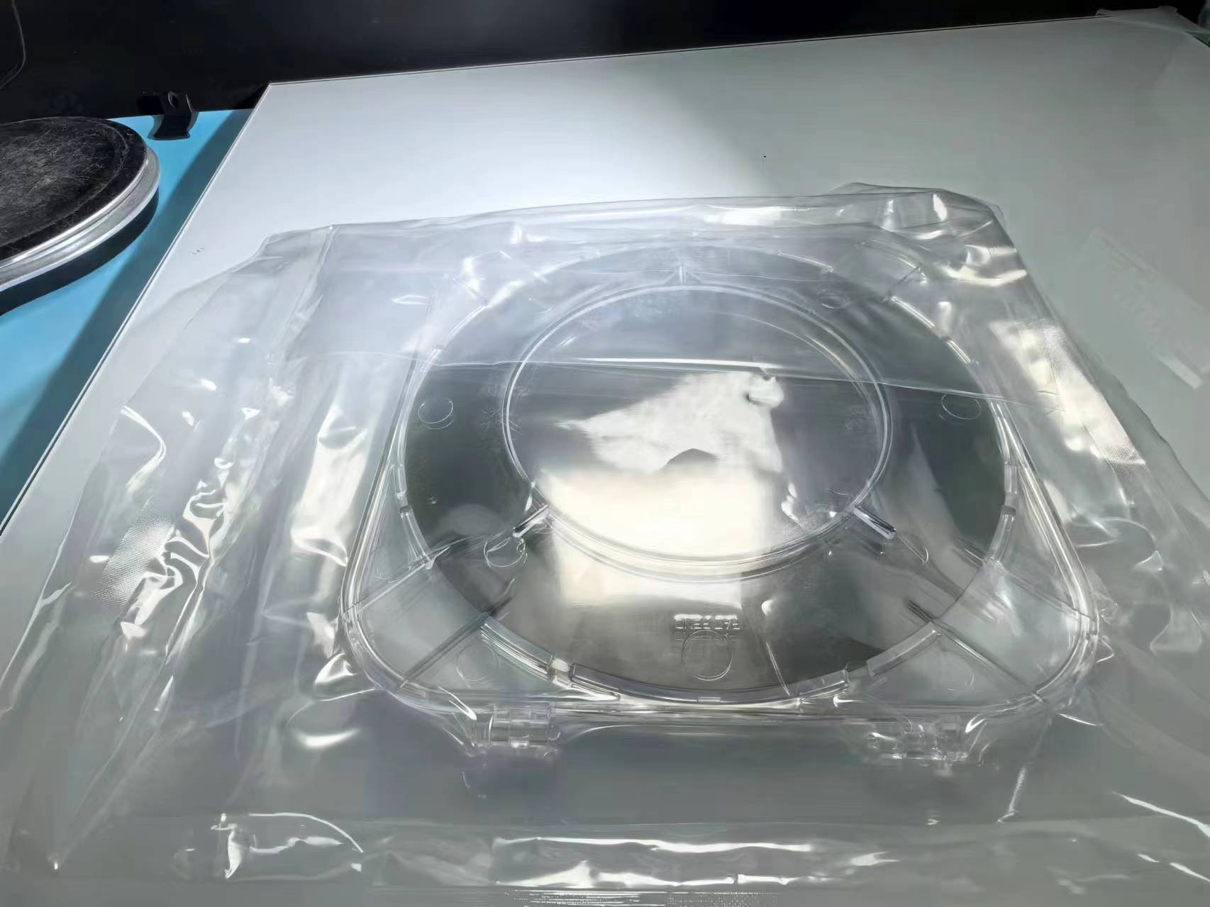
| 8.2 | packaging | -- | Multi-wafer cassette packaging |
Multi-wafer cassette packaging |
Multi-wafer cassette packaging |
Detailed Diagram
Write your message here and send it to us