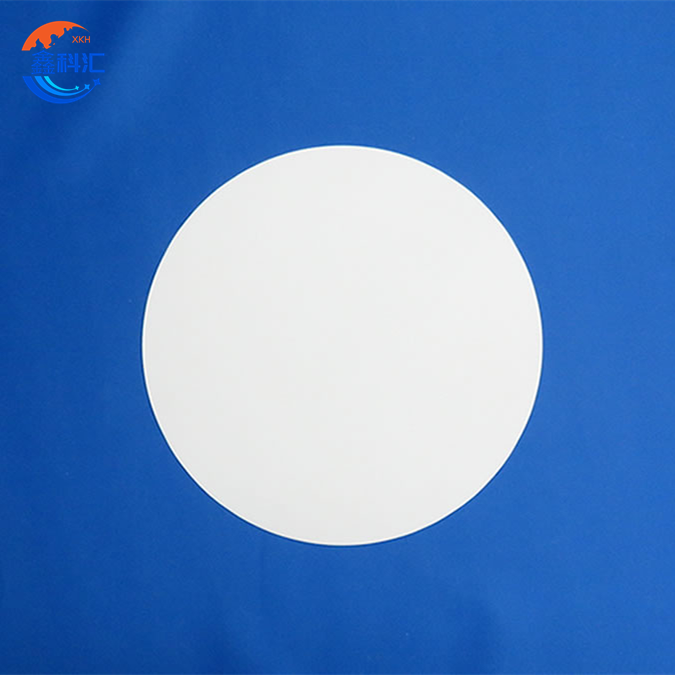
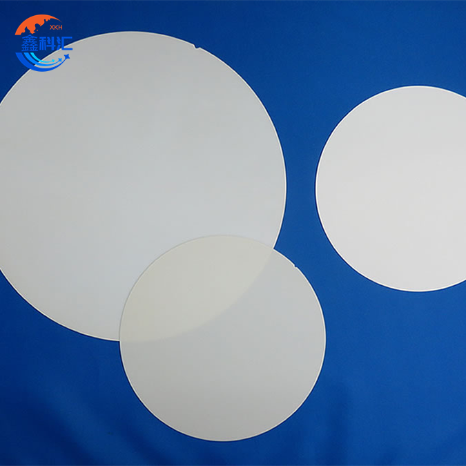
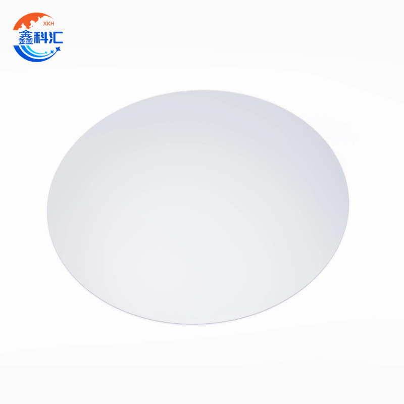
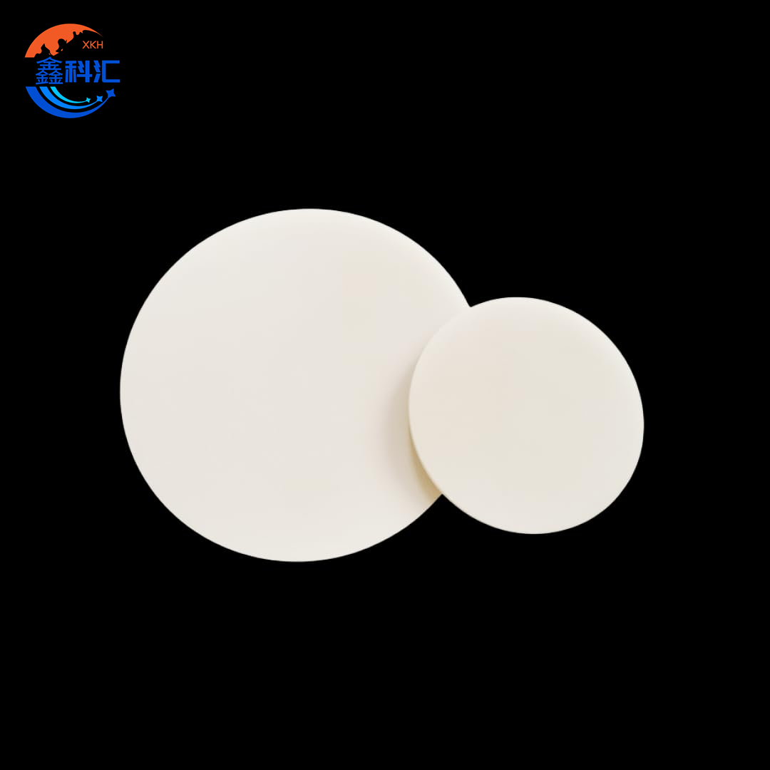
AlN on FSS 2inch 4inch NPSS/FSS AlN template for semiconductor area


Properties
Material Composition:
Aluminum Nitride (AlN) – White, high-performance ceramic layer providing excellent thermal conductivity (typically 200-300 W/m·K), good electrical insulation, and high mechanical strength.
Flexible Substrate (FSS) – Flexible polymeric films (such as Polyimide, PET, etc.) offering durability and bendability without compromising the functionality of the AlN layer.
Wafer Sizes Available:
2-inch (50.8mm)
4-inch (100mm)
Thickness:
AlN Layer: 100-2000nm
FSS Substrate Thickness: 50µm-500µm (customizable based on requirements)
Surface Finish Options:
NPSS (Non-Polished Substrate) – Unpolished substrate surface, suitable for certain applications that require rougher surface profiles for better adhesion or integration.
FSS (Flexible Substrate) – Polished or unpolished flexible film, with the option for smooth or textured surfaces, depending on the specific application needs.
Electrical Properties:
Insulating – AlN’s electrical insulating properties make it ideal for high-voltage and power semiconductor applications.
Dielectric Constant: ~9.5
Thermal Conductivity: 200-300 W/m·K (depending on specific AlN grade and thickness)
Mechanical Properties:
Flexibility: AlN is deposited on a flexible substrate (FSS) which allows for bending and flexibility.
Surface Hardness: AlN is highly durable and resists physical damage under normal operating conditions.
Applications
High-Power Devices: Ideal for power electronics requiring high thermal dissipation, such as power converters, RF amplifiers, and high-power LED modules.
RF and Microwave Components: Suitable for components like antennas, filters, and resonators where both thermal conductivity and mechanical flexibility are needed.
Flexible Electronics: Perfect for applications where devices need to conform to non-planar surfaces or require a lightweight, flexible design (e.g., wearables, flexible sensors).
Semiconductor Packaging: Used as a substrate in semiconductor packaging, offering thermal dissipation in applications that generate high heat.
LEDs and Optoelectronics: For devices that require high-temperature operation with robust heat dissipation.
Parameter Table
|
Property |
Value or Range |
| Wafer Size | 2-inch (50.8mm), 4-inch (100mm) |
| AlN Layer Thickness | 100nm – 2000nm |
| FSS Substrate Thickness | 50µm – 500µm (customizable) |
| Thermal Conductivity | 200 – 300 W/m·K |
| Electrical Properties | Insulating (Dielectric Constant: ~9.5) |
| Surface Finish | Polished or Unpolished |
| Substrate Type | NPSS (Non-Polished Substrate), FSS (Flexible Substrate) |
| Mechanical Flexibility | High flexibility, ideal for flexible electronics |
| Color | White to Off-White (depending on substrate) |
Applications
●Power Electronics: The combination of high thermal conductivity and flexibility makes these wafers perfect for power devices such as power converters, transistors, and voltage regulators that require efficient heat dissipation.
●RF/Microwave Devices: Due to AlN’s superior thermal properties and low electrical conductivity, these wafers are used in RF components like amplifiers, oscillators, and antennas.
●Flexible Electronics: The flexibility of the FSS layer combined with the excellent thermal management of AlN makes it an ideal choice for wearable electronics and sensors.
●Semiconductor Packaging: Used for high-performance semiconductor packaging where effective thermal dissipation and reliability are critical.
●LED & Optoelectronic Applications: Aluminum Nitride is an excellent material for LED packaging and other optoelectronic devices requiring high heat resistance.
Q&A (Frequently Asked Questions)
Q1: What are the benefits of using AlN on FSS wafers?
A1: AlN on FSS wafers combine the high thermal conductivity and electrical insulation properties of AlN with the mechanical flexibility of a polymer substrate. This enables improved heat dissipation in flexible electronic systems while maintaining device integrity under bending and stretching conditions.
Q2: What sizes are available for AlN on FSS wafers?
A2: We offer 2-inch and 4-inch wafer sizes. Custom sizes can be discussed upon request to meet your specific application needs.
Q3: Can I customize the thickness of the AlN layer?
A3: Yes, the AlN layer thickness can be customized, with typical ranges from 100nm to 2000nm depending on your application requirements.
Detailed Diagram