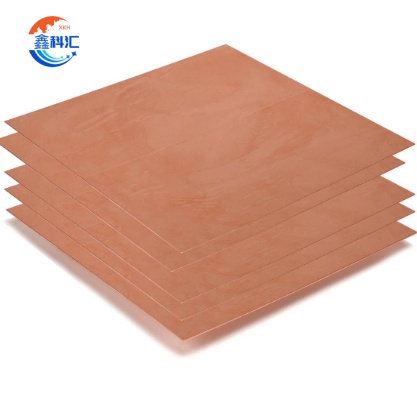
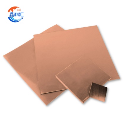
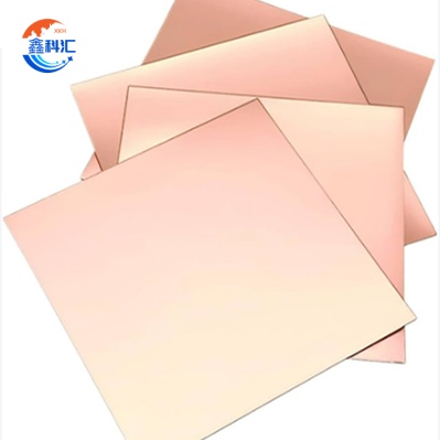
Copper substrate single crystal Cu wafer 5x5x0.5/1mm 10x10x0.5/1mm 20x20x0.5/1mm
Specification
Due to its high heat resistance and mechanical durability, copper substrates are widely used in microelectronics, heat dissipation systems and energy storage technologies, where efficient thermal management and reliability are critical. These properties make copper substrates a key material in many advanced technology applications.
These are some of the characteristics of copper single crystal substrate:Excellent electrical conductivity, conductivity second only to silver. The thermal conductivity is very good, and the thermal conductivity is the best among common metals. Good processing performance, can carry out a variety of metallurgical processing technology.Corrosion resistance is good, but some protective measures are still needed.The relative cost is low, and the price is more economical in metal substrate materials.
Copper substrate is widely used in various industries because of its excellent electrical conductivity, thermal conductivity and mechanical strength. The following are the main applications of copper substrate:
1. Electronic circuit board: copper foil substrate material as a printed circuit board (PCB). Used for high density interconnect circuit board, flexible circuit board, etc. It has good conductivity and heat dissipation properties and is suitable for high power electronic devices.
2. Thermal management applications: used as a cooling substrate for LED lamps, power electronics, etc. Manufacture various heat exchangers, radiators and other thermal management components. The excellent thermal conductivity of copper is used to conduct and dissipate heat effectively.
3. Electromagnetic shielding application: as an electronic device shell and shielding layer, to provide effective electromagnetic shielding. Used for mobile phones, computers and other electronic products of metal shell and internal shielding layer. With good electromagnetic shielding performance, can block electromagnetic interference.
4.Other applications: as a conductive circuit material for building electrical systems. Used in the manufacture of various electrical appliances, motors, transformers and other electromagnetic components. As a decorative material, make use of its good processing properties.
We can customize various specifications, thicknesses and shapes of Copper Single crystal substrate according to customers' specific requirements.
Detailed Diagram


