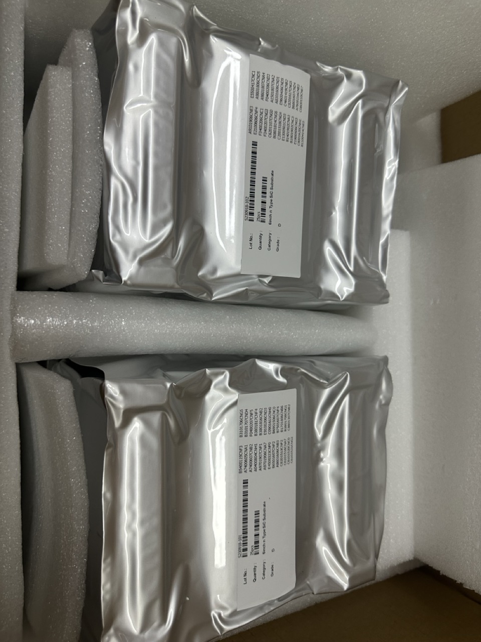
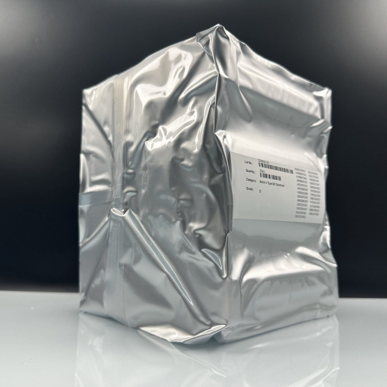
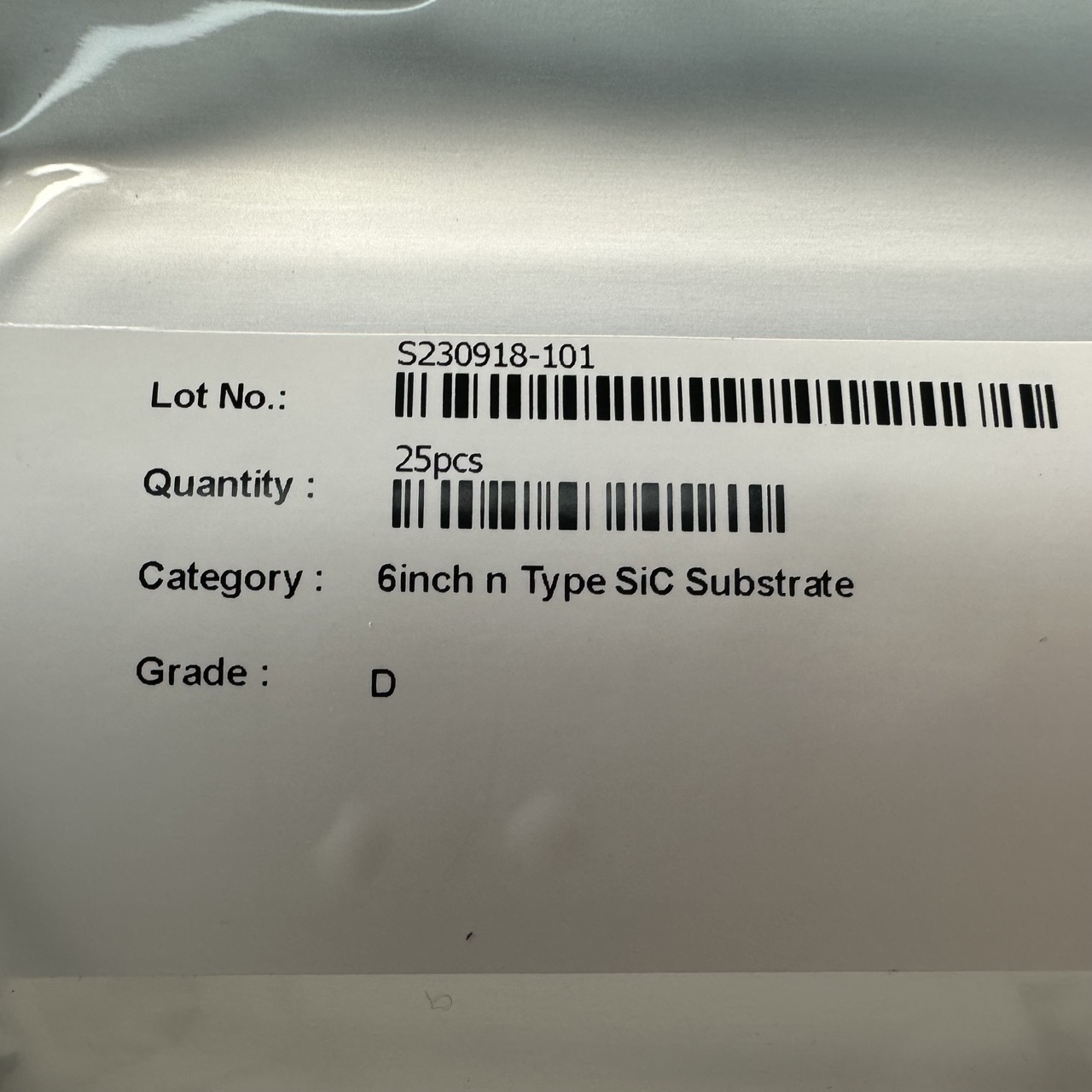
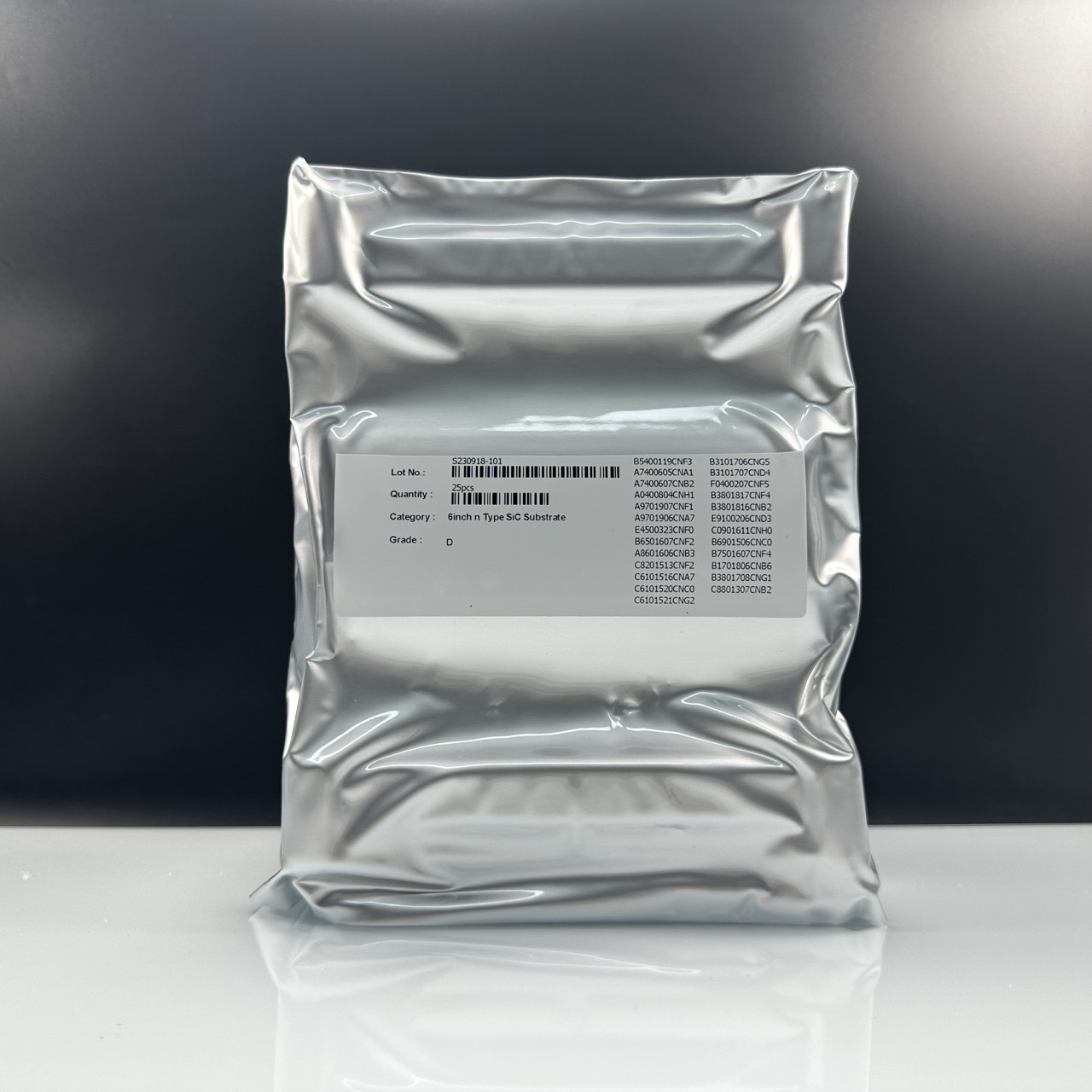
Dia150mm 4H-N 6inch SiC substrate Production and dummy grade


The main features of 6 inch silicon carbide mosfet wafers are as follows;.
High voltage withstand: Silicon carbide has a high breakdown electric field, so 6 inch silicon carbide mosfet wafers have a high voltage withstand capability, suitable for high voltage application scenarios.
High current density: Silicon carbide has a large electron mobility, making the 6-inch silicon carbide mosfet wafers have a greater current density to withstand greater current.
High operating frequency: Silicon carbide has a low carrier mobility, making the 6-inch silicon carbide mosfet wafers have a high operating frequency, suitable for high-frequency application scenarios.
Good thermal stability: Silicon carbide has a high thermal conductivity, making the 6-inch silicon carbide mosfet wafers still have good performance in high temperature environments.
6 inch silicon carbide mosfet wafers are widely used in the following areas: power electronics, including transformers, rectifiers, inverters, power amplifiers, etc., such as solar inverters, new energy vehicle charging, rail transportation, high-speed air compressor in the fuel cell, DC-DC converter (DCDC), electric vehicle motor drive and digitalization trends in the field of data centers and other areas with a wide range of applications.
We can provide 4H-N 6inch SiC substrate, different grades of substrate stock wafers. We can also arrange customization according to your needs. Welcome inquiry!
Detailed Diagram