Epi-layer
-

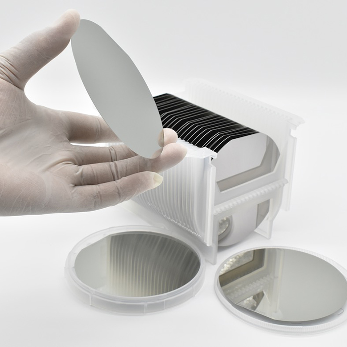
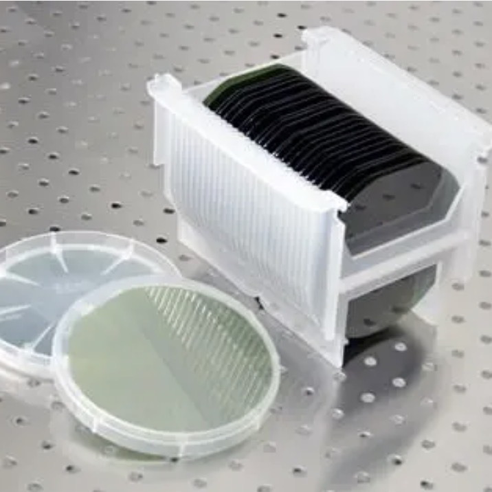
200mm 8inch GaN on sapphire Epi-layer wafer substrate
-

GaN on Glass 4-Inch: Customizable Glass Options Including JGS1, JGS2, BF33, and Ordinary Quartz
-

AlN-on-NPSS Wafer: High-Performance Aluminum Nitride Layer on Non-Polished Sapphire Substrate for High-Temperature, High-Power, and RF Applications
-

Gallium Nitride on Silicon wafer 4inch 6inch Tailored Si Substrate Orientation, Resistivity, and N-type/P-type Options
-

Customized GaN-on-SiC Epitaxial Wafers (100mm, 150mm) – Multiple SiC Substrate Options (4H-N, HPSI, 4H/6H-P)
-

GaN-on-Diamond Wafers 4inch 6inch Total epi thickness (micron) 0.6 ~ 2.5 or customized for High-Frequency Applications
-

GaAs high-power epitaxial wafer substrate gallium arsenide wafer power laser wavelength 905nm for laser medical treatment
-

InGaAs epitaxial wafer substrate PD Array photodetector arrays can be used for LiDAR
-

2inch 3inch 4inch InP epitaxial wafer substrate APD light detector for fiber optic communications or LiDAR
-
Silicon-On-Insulator Substrate SOI wafer three layers for Microelectronics and Radio Frequency
-

SOI wafer insulator on silicon 8-inch and 6-inch SOI (Silicon-On-Insulator) wafers
-
6inch SiC Epitaxiy wafer N/P type accept customized