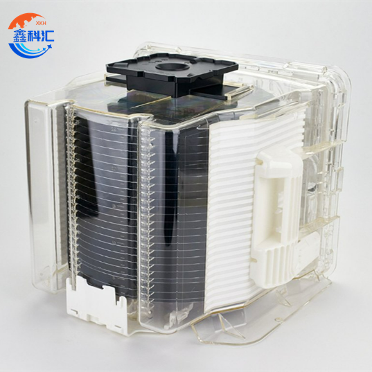
FOSB wafer carrier box 25slots for 12inch wafer Precision spacing for Automated operations Ultra-clean materials


Key Features
|
Feature |
Description |
| Slot Capacity | 25 slots for 12-inch wafers, maximizing the storage space while ensuring wafers are securely held. |
| Automated Handling | Designed for automated wafer handling, reducing human error and increasing efficiency in semiconductor fabs. |
| Precision Slot Spacing | Precision-engineered slot spacing prevents wafer contact, reducing the risk of contamination and mechanical damage. |
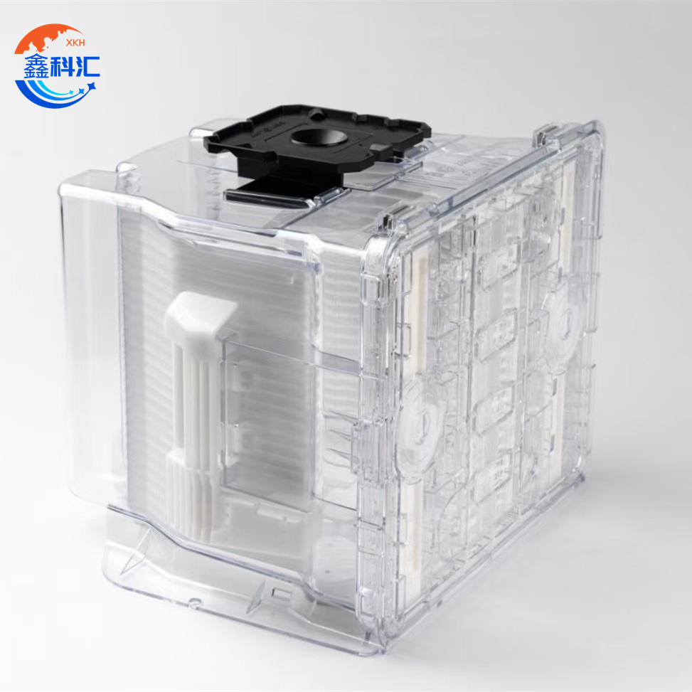
| Ultra-Clean Materials | Crafted from ultra-clean, low-outgassing materials to maintain the integrity of wafers and minimize contamination. |
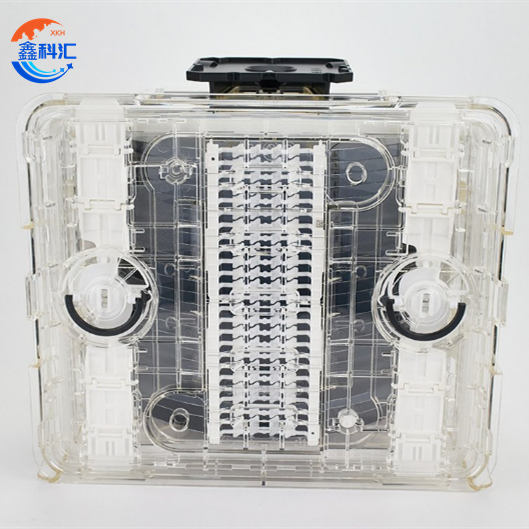
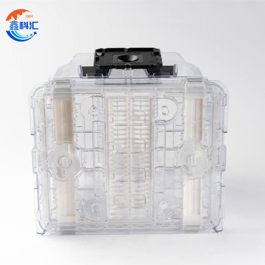
| Wafer Retention System | Incorporates a high-performance wafer retention system to keep wafers securely in place during transport. |
| SEMI/FIMS & AMHS Compliance | Fully SEMI/FIMS and AMHS compliant, ensuring seamless integration into automated semiconductor systems. |
| Particle Control | Designed to minimize particle generation, providing a cleaner environment for wafer transport. |
| Customizable Design | Customizable to meet specific production needs, including adjustments to slot configurations or material choices. |
| High Durability | Constructed from high-strength materials to withstand the rigors of transport without compromising functionality. |
Detailed Features
1.25-Slot Capacity for 12-inch Wafers
The 25-slot FOSB is designed to securely hold up to 12-inch wafers, allowing for safe and efficient transport. Each slot is carefully engineered to ensure precise wafer alignment and stability, reducing the risk of wafer breakage or deformation. The design optimizes space while maintaining safe distances between wafers, essential for preventing damage during transport or handling.
2.Precision Spacing for Damage Prevention
The precision spacing between slots is meticulously calculated to prevent direct contact between wafers. This feature is crucial in semiconductor wafer handling, as even a minor scratch or contamination can cause significant defects. By ensuring adequate space between wafers, the FOSB box minimizes the potential for physical damage and contamination during transport, storage, and handling.
3.Designed for Automated Operations
The FOSB wafer carrier box is optimized for automated operations, reducing the need for human intervention in the wafer transport process. By integrating seamlessly with automated material handling systems (AMHS), the box enhances operational efficiency, reduces the risk of contamination from human contact, and accelerates wafer transport between processing areas. This compatibility ensures smoother and faster wafer handling in modern semiconductor production environments.
4.Ultra-Clean, Low-Outgassing Materials
To ensure the highest levels of cleanliness, the FOSB wafer carrier box is made from ultra-clean, low-outgassing materials. This construction prevents the release of volatile compounds that could compromise wafer integrity, ensuring that wafers remain uncontaminated during transport and storage. This feature is particularly critical in semiconductor fabs where even the smallest particles or chemical contaminants can lead to costly defects.
5.Robust Wafer Retention System
The wafer retention system within the FOSB box ensures that wafers are securely held in place during transport, preventing any movement that could lead to wafer misalignment, scratches, or other forms of damage. This system is engineered to maintain wafer position even in high-speed automated environments, offering superior protection for delicate wafers.
6.Particle Control and Cleanliness
The design of the FOSB wafer carrier box focuses on minimizing particle generation, which is one of the leading causes of wafer defects in semiconductor production. By using ultra-clean materials and a robust retention system, the FOSB box helps to keep contamination levels to a minimum, maintaining the cleanliness required for semiconductor production.
7.SEMI/FIMS and AMHS Compliance
The FOSB wafer carrier box meets SEMI/FIMS and AMHS standards, ensuring it is fully compatible with industry-standard automated material handling systems. This compliance ensures the box is compatible with the stringent requirements of semiconductor manufacturing facilities, facilitating smooth integration into production workflows and boosting operational efficiency.
8.Durability and Longevity
Made from high-strength materials, the FOSB wafer carrier box is designed to withstand the physical demands of wafer transport while maintaining its structural integrity. This durability ensures that the box can be used repeatedly in high-throughput environments without the need for frequent replacements, offering a cost-effective solution in the long term.
9.Customizable for Unique Needs
The FOSB wafer carrier box offers customization options to meet specific operational needs. Whether it’s adjusting the number of slots, changing the box’s dimensions, or selecting special materials for particular applications, the carrier box can be tailored to suit a wide range of semiconductor production requirements.
Applications
The 12-inch (300mm) FOSB wafer carrier box is ideal for a variety of applications within semiconductor manufacturing and related fields:
Semiconductor Wafer Handling
The box ensures secure and efficient handling of 12-inch wafers during all stages of production, from initial fabrication to final testing and packaging. Its automated handling and precision slot spacing protect wafers from contamination and mechanical damage, ensuring a high yield in semiconductor manufacturing.
Wafer Storage
In semiconductor fabs, wafer storage must be handled with care to avoid degradation or contamination. The FOSB carrier box provides a stable and clean environment, protecting wafers during storage and helping to maintain their integrity until they are ready for further processing.
Transporting Wafers Between Production Stages
The FOSB wafer carrier box is designed to safely transport wafers between different stages of production, reducing the risk of wafer damage during transit. Whether moving wafers within the same fab or between different facilities, the carrier box ensures wafers are transported safely and efficiently.
Integration with AMHS
The FOSB wafer carrier box integrates seamlessly with automated material handling systems (AMHS), enabling high-speed wafer movement within modern semiconductor fabs. The automation provided by AMHS improves efficiency, reduces human errors, and increases overall throughput in semiconductor production lines.
FOSB Keywords Q&A
Q1: How many wafers can the FOSB carrier box hold?
A1: The FOSB wafer carrier box has a 25-slot capacity, specifically designed to hold 12-inch (300mm) wafers securely during handling, storage, and transport.
Q2: What are the benefits of precision spacing in the FOSB carrier box?
A2: Precision spacing ensures that wafers are kept at a safe distance from one another, preventing contact that could lead to scratches, cracks, or contamination. This feature is critical for preserving the integrity of the wafers throughout the transport and handling process.
Q3: Can the FOSB box be used with automated systems?
A3: Yes, the FOSB wafer carrier box is optimized for automated operations and is fully compatible with AMHS, making it ideal for high-speed, automated semiconductor production lines.
Q4: What materials are used in the FOSB carrier box to prevent contamination?
A4: The FOSB carrier box is made from ultra-clean, low-outgassing materials, which are carefully chosen to prevent contamination and ensure wafer integrity during transport and storage.
Q5: How does the wafer retention system work in the FOSB box?
A5: The wafer retention system secures the wafers in place, preventing any movement during transport, even in high-speed automated systems. This system minimizes the risk of wafer misalignment or damage due to vibrations or external forces.
Q6: Can the FOSB wafer carrier box be customized for specific needs?
A6: Yes, the FOSB wafer carrier box offers customization options, allowing adjustments to slot configurations, materials, and dimensions to meet the unique requirements of semiconductor fabs.
Conclusion
The 12-inch (300mm) FOSB wafer carrier box offers a highly secure and efficient solution for semiconductor wafer transport and storage. With 25 slots, precision spacing, ultra-clean materials, and compatibility with
Detailed Diagram