GaN-on-Diamond Wafers 4inch 6inch Total epi thickness (micron) 0.6 ~ 2.5 or customized for High-Frequency Applications


Properties
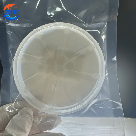
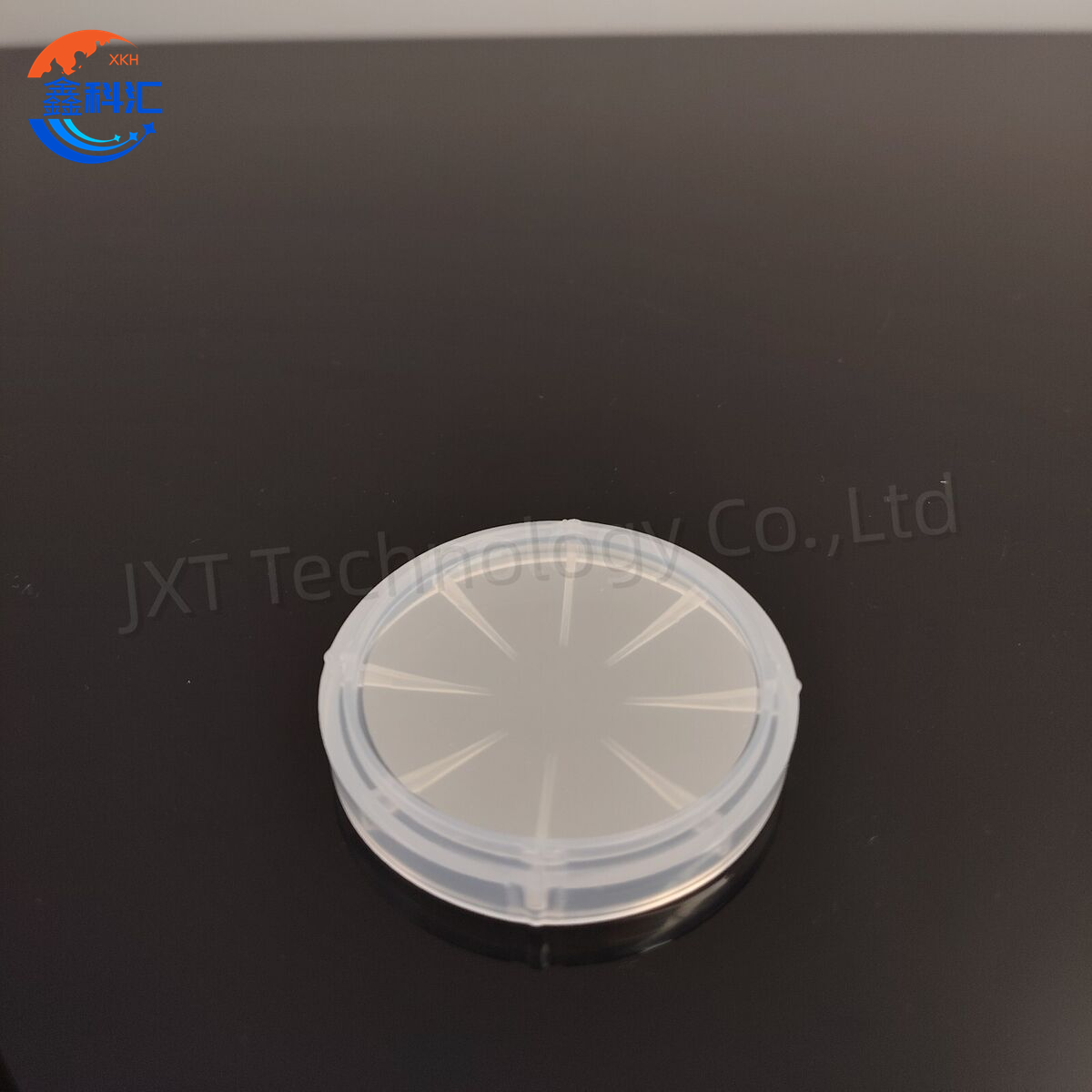
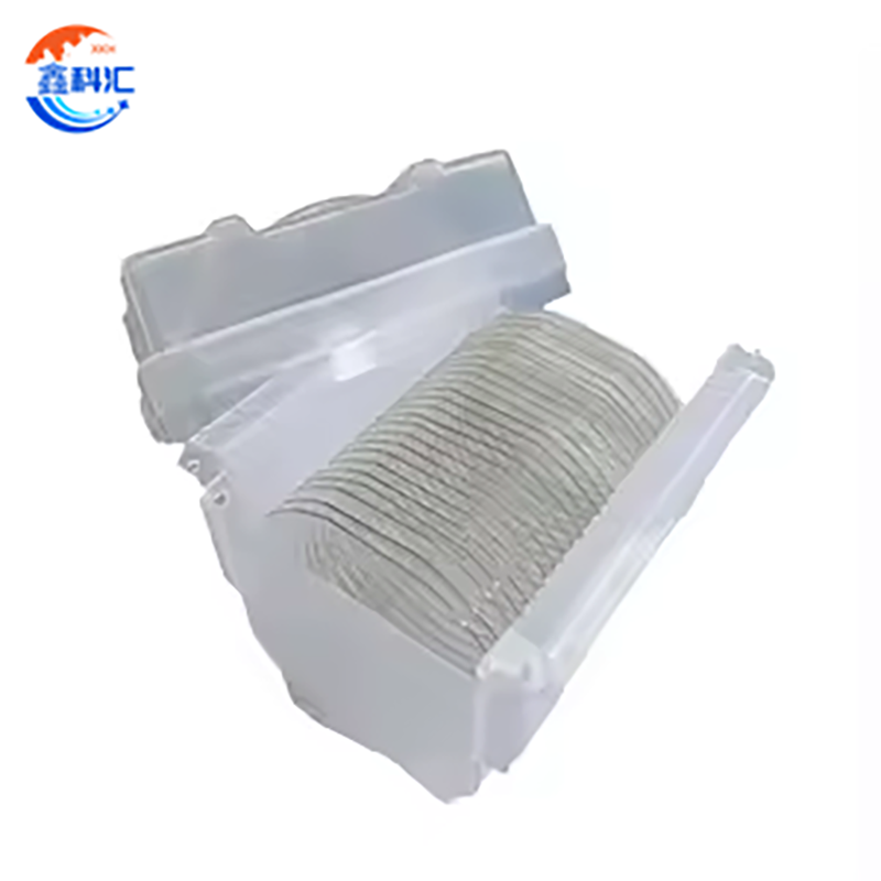
Wafer Size:
Available in 4-inch and 6-inch diameters for versatile integration into various semiconductor manufacturing processes.
Customization options available for wafer size, depending on customer requirements.
Epitaxial Layer Thickness:
Range: 0.6 µm to 2.5 µm, with options for customized thicknesses based on specific application needs.
The epitaxial layer is designed to ensure high-quality GaN crystal growth, with optimized thickness to balance power, frequency response, and thermal management.
Thermal Conductivity:
Diamond layer provides an extremely high thermal conductivity of approximately 2000-2200 W/m·K, ensuring efficient heat dissipation from high-power devices.
GaN Material Properties:
Wide Bandgap: The GaN layer benefits from a wide bandgap (~3.4 eV), which allows for operation in harsh environments, high voltage, and high-temperature conditions.
Electron Mobility: High electron mobility (approx. 2000 cm²/V·s), leading to faster switching and higher operational frequencies.
High Breakdown Voltage: GaN's breakdown voltage is much higher than conventional semiconductor materials, making it suitable for power-intensive applications.
Electrical Performance:
High Power Density: GaN-on-Diamond wafers enable high power output while maintaining a small form factor, perfect for power amplifiers and RF systems.
Low Losses: The combination of GaN's efficiency and diamond's heat dissipation leads to lower power losses during operation.
Surface Quality:
High-Quality Epitaxial Growth: The GaN layer is epitaxially grown on the diamond substrate, ensuring minimal dislocation density, high crystalline quality, and optimal device performance.
Uniformity:
Thickness and Composition Uniformity: Both the GaN layer and the diamond substrate maintain excellent uniformity, critical for consistent device performance and reliability.
Chemical Stability:
Both GaN and diamond offer exceptional chemical stability, allowing these wafers to perform reliably in harsh chemical environments.
Applications
RF Power Amplifiers:
GaN-on-Diamond wafers are ideal for RF power amplifiers in telecommunications, radar systems, and satellite communications, offering both high efficiency and reliability at high frequencies (e.g., 2 GHz to 20 GHz and beyond).
Microwave Communication:
These wafers excel in microwave communication systems, where high power output and minimal signal degradation are critical.
Radar and Sensing Technologies:
GaN-on-Diamond wafers are widely used in radar systems, providing robust performance in high-frequency and high-power applications, especially in military, automotive, and aerospace sectors.
Satellite Systems:
In satellite communication systems, these wafers ensure the durability and high performance of power amplifiers, capable of operating in extreme environmental conditions.
High-Power Electronics:
The thermal management capabilities of GaN-on-Diamond make them suitable for high-power electronics, such as power converters, inverters, and solid-state relays.
Thermal Management Systems:
Due to the high thermal conductivity of diamond, these wafers can be used in applications requiring robust thermal management, such as high-power LED and laser systems.
Q&A for GaN-on-Diamond Wafers
Q1: What is the advantage of using GaN-on-Diamond wafers in high-frequency applications?
A1: GaN-on-Diamond wafers combine the high electron mobility and wide bandgap of GaN with the outstanding thermal conductivity of diamond. This enables high-frequency devices to operate at higher power levels while effectively managing heat, ensuring greater efficiency and reliability compared to traditional materials.
Q2: Can GaN-on-Diamond wafers be customized for specific power and frequency requirements?
A2: Yes, GaN-on-Diamond wafers offer customizable options, including epitaxial layer thickness (0.6 µm to 2.5 µm), wafer size (4-inch, 6-inch), and other parameters based on specific application needs, providing flexibility for high-power and high-frequency applications.
Q3: What are the key benefits of diamond as a substrate for GaN?
A3: Diamond's extreme thermal conductivity (up to 2200 W/m·K) helps efficiently dissipate heat generated by high-power GaN devices. This thermal management capability allows GaN-on-Diamond devices to operate at higher power densities and frequencies, ensuring improved device performance and longevity.
Q4: Are GaN-on-Diamond wafers suitable for space or aerospace applications?
A4: Yes, GaN-on-Diamond wafers are well-suited for space and aerospace applications due to their high reliability, thermal management capabilities, and performance in extreme conditions, such as high radiation, temperature variations, and high-frequency operation.
Q5: What is the expected lifespan of devices made from GaN-on-Diamond wafers?
A5: The combination of GaN's inherent durability and diamond's exceptional heat dissipation properties results in a long lifespan for devices. GaN-on-Diamond devices are designed to operate in harsh environments and high-power conditions with minimal degradation over time.
Q6: How does the thermal conductivity of diamond affect the overall performance of GaN-on-Diamond wafers?
A6: The high thermal conductivity of diamond plays a critical role in enhancing the performance of GaN-on-Diamond wafers by efficiently conducting away the heat generated in high-power applications. This ensures that the GaN devices maintain optimal performance, reduce thermal stress, and avoid overheating, which is a common challenge in conventional semiconductor devices.
Q7: What are the typical applications where GaN-on-Diamond wafers outperform other semiconductor materials?
A7: GaN-on-Diamond wafers outperform other materials in applications requiring high power handling, high-frequency operation, and efficient thermal management. This includes RF power amplifiers, radar systems, microwave communication, satellite communication, and other high-power electronics.
Conclusion
GaN-on-Diamond wafers offer a unique solution for high-frequency and high-power applications, combining the high performance of GaN with the exceptional thermal properties of diamond. With customizable features, they are designed to meet the needs of industries requiring efficient power delivery, thermal management, and high-frequency operation, ensuring reliability and longevity in challenging environments.
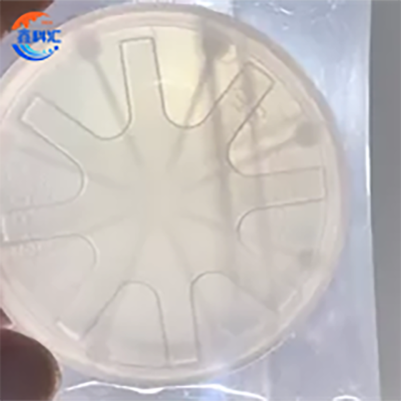
Detailed Diagram