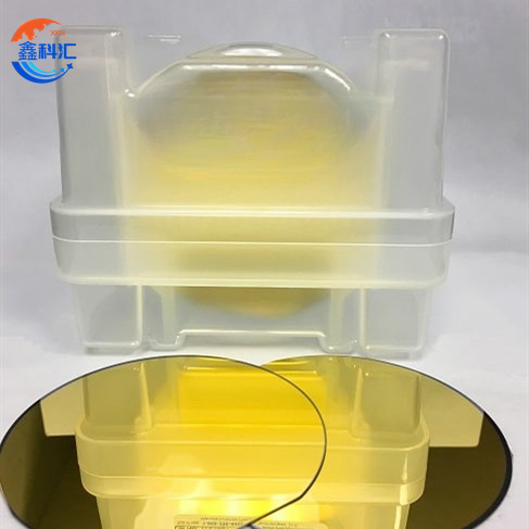
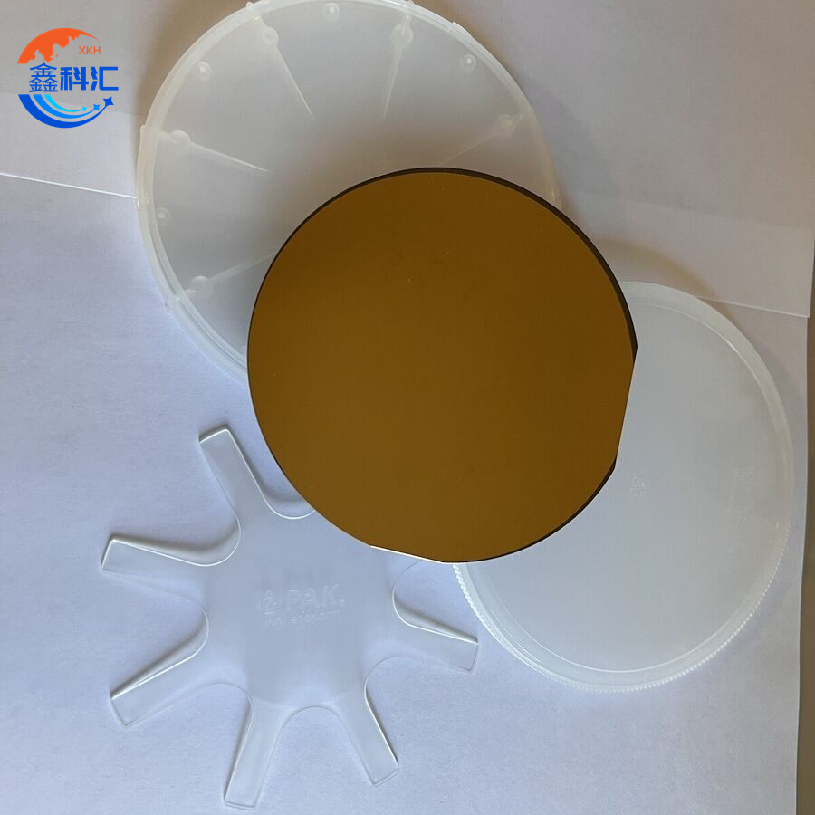
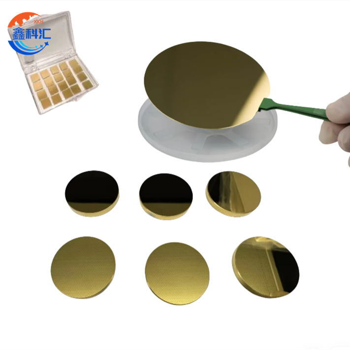
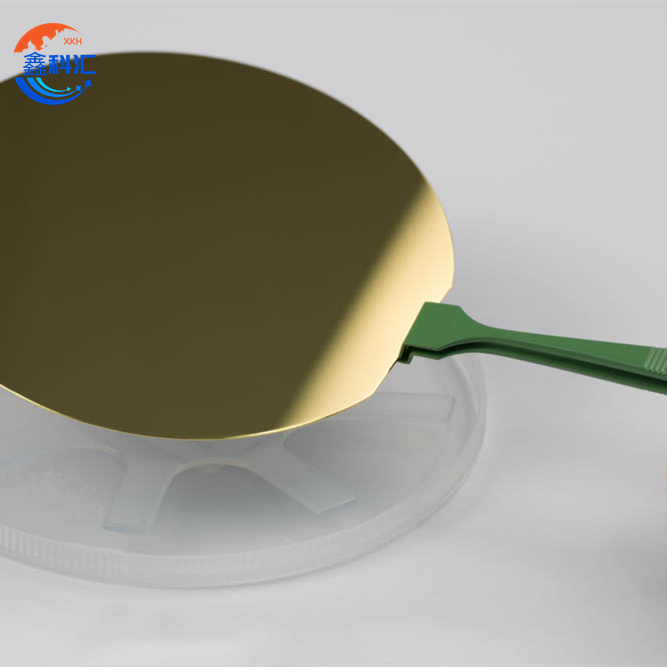
gold plate silicon wafer (Si Wafer)10nm 50nm 100nm 500nm Au Excellent Conductivity for LED


Key Features
|
Feature |
Description |
| Wafer Diameter | Available in 2-inch, 4-inch, 6-inch |
| Gold Layer Thickness | 50nm (±5nm) or customizable for specific needs |
| Gold Purity | 99.999% Au (high purity for optimal performance) |
| Coating Method | Electroplating or vacuum deposition for uniform coating |
| Surface Finish | Smooth, defect-free surface, essential for precision applications |
| Thermal Conductivity | High thermal conductivity for effective heat dissipation |
| Electrical Conductivity | Superior electrical conductivity, ideal for semiconductor use |
| Corrosion Resistance | Excellent resistance to oxidation, ideal for harsh environments |
Why Gold Coating is Essential in the Semiconductor Industry
Electrical Conductivity
Gold is known for its superior electrical conductivity, making it ideal for applications where efficient and stable electrical connections are needed. In semiconductor manufacturing, gold-coated wafers provide highly reliable interconnections and reduce signal degradation.
Corrosion Resistance
Unlike other metals, gold does not oxidize or corrode over time, making it an excellent choice for protecting sensitive electrical contacts. In semiconductor packaging and devices exposed to harsh environmental conditions, the corrosion resistance of gold ensures that connections remain intact and functional for long periods.
Thermal Management
The thermal conductivity of gold is very high, ensuring that the gold-coated silicon wafer can effectively dissipate heat generated by the semiconductor device. This is crucial in preventing device overheating and maintaining optimal performance.
Mechanical Strength and Durability
Gold coatings add mechanical strength to silicon wafers, preventing surface damage and improving the wafer's durability during processing, transport, and handling.
Post-Coating Characteristics
Enhanced Surface Quality
The gold-coated wafer offers a smooth, uniform surface that is critical for high-precision applications like semiconductor manufacturing, where defects on the surface can affect the performance of the final product.
Superior Bonding and Soldering Properties
The gold coating makes the silicon wafer ideal for wire bonding, flip-chip bonding, and soldering in semiconductor devices, ensuring secure and stable electrical connections.
Long-Term Stability
Gold-coated wafers provide enhanced long-term stability in semiconductor applications. The gold layer protects the wafer from oxidation and damage, ensuring the wafer performs reliably over time, even in extreme environments.
Improved Device Reliability
By reducing the risk of failure from corrosion or heat, gold-coated silicon wafers contribute significantly to the reliability and longevity of semiconductor devices and systems.
Parameters
|
Property |
Value |
| Wafer Diameter | 2-inch, 4-inch, 6-inch |
| Gold Layer Thickness | 50nm (±5nm) or customizable |
| Gold Purity | 99.999% Au |
| Coating Method | Electroplating or vacuum deposition |
| Surface Finish | Smooth, defect-free |
| Thermal Conductivity | 315 W/m·K |
| Electrical Conductivity | 45.5 x 10⁶ S/m |
| Density of Gold | 19.32 g/cm³ |
| Melting Point of Gold | 1064°C |
Applications of Gold-Coated Silicon Wafers
Semiconductor Packaging
Gold-coated wafers are crucial for IC packaging in advanced semiconductor devices, offering superior electrical connections and enhanced thermal performance.
LED Manufacturing
In LED production, the gold layer provides effective heat dissipation and electrical conductivity, ensuring better performance and longevity for high-power LEDs.
Optoelectronics
Gold-coated wafers are used in the manufacturing of optoelectronic devices, such as photodetectors, lasers, and light sensors, where stable electrical and thermal management is critical.
Photovoltaic Applications
Gold-coated wafers are also used in solar cells, where their corrosion resistance and high conductivity improve overall device efficiency and performance.
Microelectronics and MEMS
In MEMS (Micro-Electromechanical Systems) and other microelectronics, gold-coated wafers ensure precise electrical connections and contribute to the long-term stability and reliability of the devices.
Frequently Asked Questions (Q&A)
Q1: Why use gold to coat silicon wafers?
A1: Gold is chosen due to its excellent electrical conductivity, corrosion resistance, and thermal properties, which are critical for semiconductor applications that require reliable electrical connections, efficient heat dissipation, and long-term durability.
Q2: What is the standard gold layer thickness?
A2: The standard gold layer thickness is 50nm (±5nm), but custom thicknesses can be tailored to meet specific needs depending on the application.
Q3: How does gold improve wafer performance?
A3: The gold layer enhances electrical conductivity, thermal dissipation, and corrosion resistance, all of which are essential for improving the reliability and performance of semiconductor devices.
Q4: Can the wafer sizes be customized?
A4: Yes, we offer 2-inch, 4-inch, and 6-inch diameters as standard, but we also provide customized wafer sizes upon request.
Q5: What applications benefit from gold-coated wafers?
A5: Gold-coated wafers are ideal for semiconductor packaging, LED manufacturing, optoelectronics, MEMS, and solar cells, among other precision applications that require high performance.
Q6: What is the main benefit of using gold for bonding in semiconductor manufacturing?
A6: Gold's excellent solderability and bonding properties make it perfect for creating reliable interconnects in semiconductor devices, ensuring long-lasting electrical connections with minimal resistance.
Conclusion
Our Gold Coated Silicon Wafers provide a high-performance solution for the semiconductor, optoelectronics, and microelectronics industries. With 99.999% pure gold coating, these wafers offer exceptional electrical conductivity, thermal dissipation, and corrosion resistance, ensuring enhanced reliability and performance in a wide range of applications, from LEDs and ICs to photovoltaic devices. Whether for soldering, bonding, or packaging, these wafers are the ideal choice for your high-precision needs.
Detailed Diagram