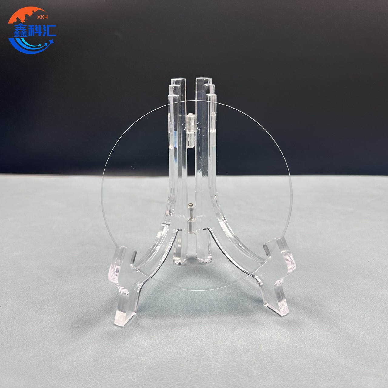
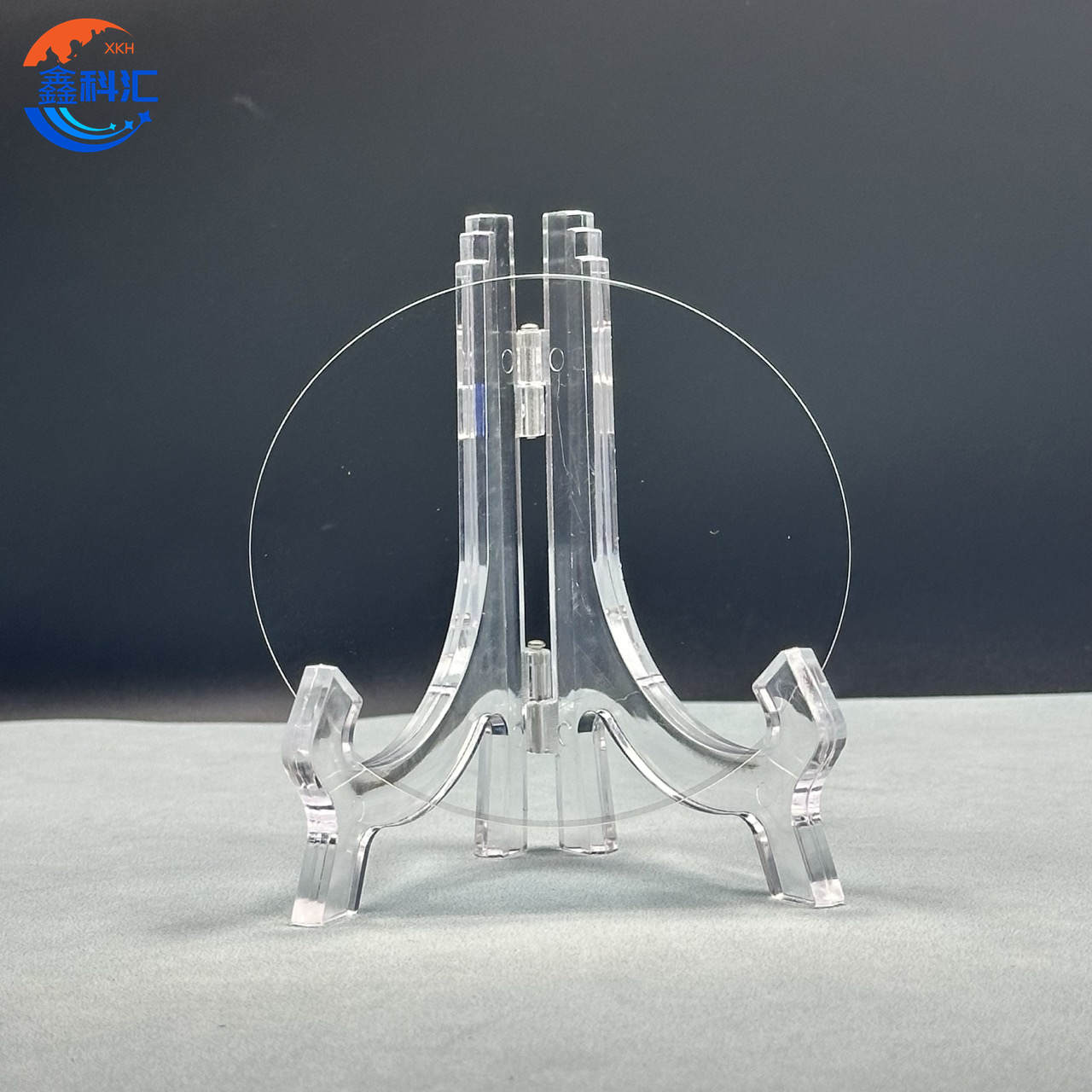
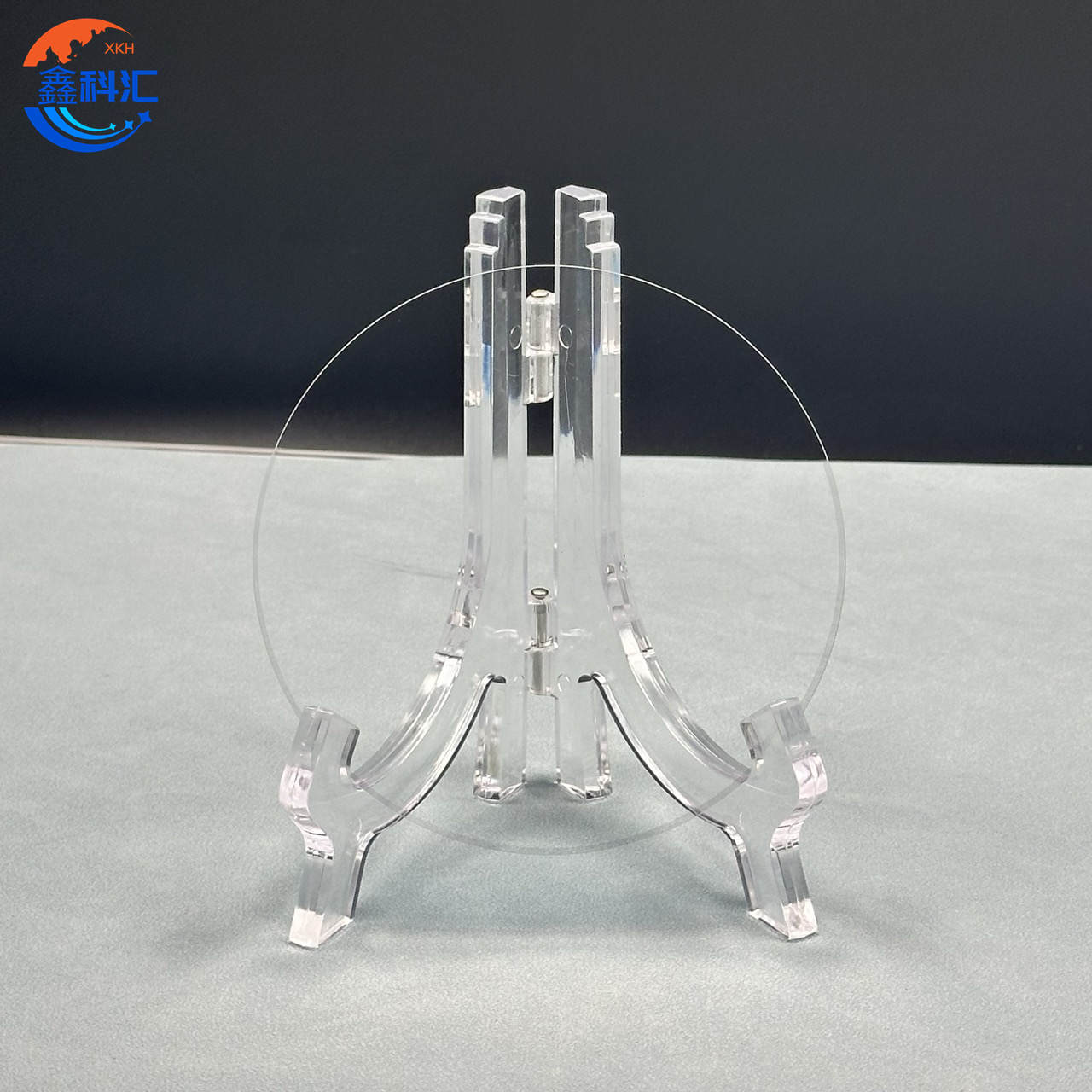
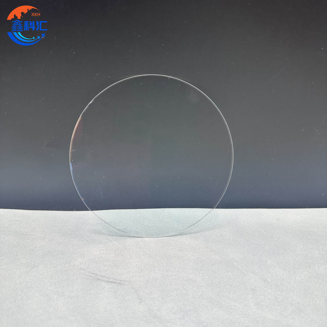
HPSI SiC wafer dia:3inch thickness:350um± 25 µm for Power Electronics
Application
HPSI SiC wafers are used in a wide range of power electronics applications, including:
Power Semiconductors: SiC wafers are commonly employed in the production of power diodes, transistors (MOSFETs, IGBTs), and thyristors. These semiconductors are widely used in power conversion applications that require high efficiency and reliability, such as in industrial motor drives, power supplies, and inverters for renewable energy systems.
Electric Vehicles (EVs): In electric vehicle powertrains, SiC-based power devices provide faster switching speeds, higher energy efficiency, and reduced thermal losses. SiC components are ideal for applications in battery management systems (BMS), charging infrastructure, and on-board chargers (OBCs), where minimizing weight and maximizing energy conversion efficiency is critical.
Renewable Energy Systems: SiC wafers are increasingly used in solar inverters, wind turbine generators, and energy storage systems, where high efficiency and robustness are essential. SiC-based components enable higher power density and enhanced performance in these applications, improving the overall energy conversion efficiency.
Industrial Power Electronics: In high-performance industrial applications, such as motor drives, robotics, and large-scale power supplies, the use of SiC wafers allows for improved performance in terms of efficiency, reliability, and thermal management. SiC devices can handle high switching frequencies and high temperatures, making them suitable for demanding environments.
Telecommunications and Data Centers: SiC is used in power supplies for telecommunications equipment and data centers, where high reliability and efficient power conversion are crucial. SiC-based power devices enable higher efficiency at smaller sizes, which translates into reduced power consumption and better cooling efficiency in large-scale infrastructures.
The high breakdown voltage, low on-resistance, and excellent thermal conductivity of SiC wafers make them the ideal substrate for these advanced applications, enabling the development of next-generation energy-efficient power electronics.
Properties
|
Property |
Value |
| Wafer Diameter | 3 inches (76.2 mm) |
| Wafer Thickness | 350 µm ± 25 µm |
| Wafer Orientation | <0001> on-axis ± 0.5° |
| Micropipe Density (MPD) | ≤ 1 cm⁻² |
| Electrical Resistivity | ≥ 1E7 Ω·cm |
| Dopant | Undoped |
| Primary Flat Orientation | {11-20} ± 5.0° |
| Primary Flat Length | 32.5 mm ± 3.0 mm |
| Secondary Flat Length | 18.0 mm ± 2.0 mm |
| Secondary Flat Orientation | Si face up: 90° CW from primary flat ± 5.0° |
| Edge Exclusion | 3 mm |
| LTV/TTV/Bow/Warp | 3 µm / 10 µm / ±30 µm / 40 µm |
| Surface Roughness | C-face: Polished, Si-face: CMP |
| Cracks (inspected by high intensity light) | None |
| Hex Plates (inspected by high intensity light) | None |
| Polytype Areas (inspected by high intensity light) | Cumulative area 5% |
| Scratches (inspected by high intensity light) | ≤ 5 scratches, cumulative length ≤ 150 mm |
| Edge Chipping | None permitted ≥ 0.5 mm width and depth |
| Surface Contamination (inspected by high intensity light) | None |
Key Benefits
High Thermal Conductivity: SiC wafers are known for their exceptional ability to dissipate heat, which allows power devices to operate at higher efficiencies and handle higher currents without overheating. This feature is crucial in power electronics where heat management is a significant challenge.
High Breakdown Voltage: The wide bandgap of SiC enables devices to tolerate higher voltage levels, making them ideal for high-voltage applications such as power grids, electric vehicles, and industrial machinery.
High Efficiency: The combination of high switching frequencies and low on-resistance results in devices with lower energy loss, improving the overall efficiency of power conversion and reducing the need for complex cooling systems.
Reliability in Harsh Environments: SiC is capable of operating at high temperatures (up to 600°C), which makes it suitable for use in environments that would otherwise damage traditional silicon-based devices.
Energy Savings: SiC power devices improve energy conversion efficiency, which is critical in reducing power consumption, especially in large systems like industrial power converters, electric vehicles, and renewable energy infrastructure.
Detailed Diagram


