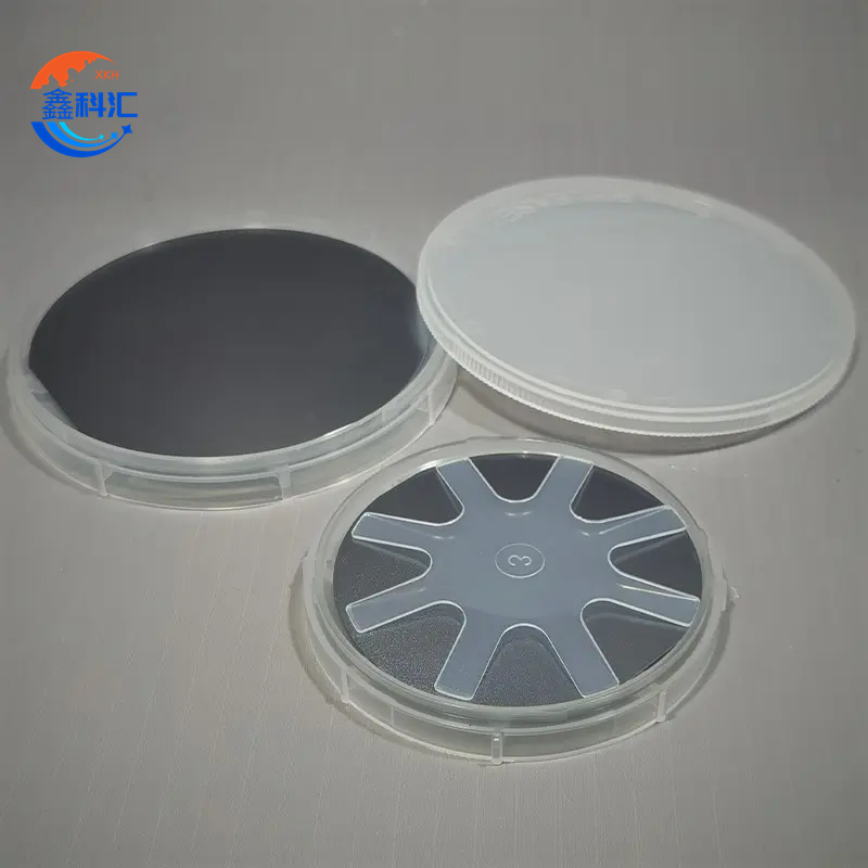
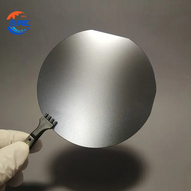
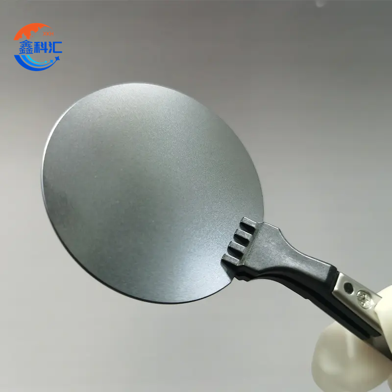
Indium Antimonide (InSb) wafers N type P type Epi ready undoped Te doped or Ge doped 2inch 3inch 4inch thickness Indium Antimonide (InSb) wafers
Features
Doping Options:
1.Undoped: These wafers are free from any doping agents, making them ideal for specialized applications such as epitaxial growth.
2.Te Doped (N-Type): Tellurium (Te) doping is commonly used to create N-type wafers, which are ideal for applications such as infrared detectors and high-speed electronics.
3.Ge Doped (P-Type): Germanium (Ge) doping is used to create P-type wafers, offering high hole mobility for advanced semiconductor applications.
Size Options:
1.Available in 2-inch, 3-inch, and 4-inch diameters. These wafers cater to different technological needs, from research and development to large-scale manufacturing.
2.Precise diameter tolerances ensure consistency across batches, with diameters of 50.8±0.3mm (for 2-inch wafers) and 76.2±0.3mm (for 3-inch wafers).
Thickness Control:
1.The wafers are available with a thickness of 500±5μm for optimal performance in various applications.
2.Additional measurements such as TTV (Total Thickness Variation), BOW, and Warp are carefully controlled to ensure high uniformity and quality.
Surface Quality:
1.The wafers come with a polished/etched surface for improved optical and electrical performance.
2.These surfaces are ideal for epitaxial growth, offering a smooth base for further processing in high-performance devices.
Epi-Ready:
1.The InSb wafers are epi-ready, meaning they are pre-treated for epitaxial deposition processes. This makes them ideal for applications in semiconductor manufacturing where epitaxial layers need to be grown on top of the wafer.
Applications
1.Infrared Detectors: InSb wafers are commonly used in infrared (IR) detection, particularly in the mid-wavelength infrared (MWIR) range. These wafers are essential for night vision, thermal imaging, and infrared spectroscopy applications.
2.High-Speed Electronics: Due to their high electron mobility, InSb wafers are used in high-speed electronic devices such as high-frequency transistors, quantum well devices, and high-electron mobility transistors (HEMTs).
3.Quantum Well Devices: The narrow bandgap and excellent electron mobility make InSb wafers suitable for use in quantum well devices. These devices are key components in lasers, detectors, and other optoelectronic systems.
4.Spintronic Devices: InSb is also being explored in spintronic applications, where electron spin is used for information processing. The material's low spin-orbit coupling makes it ideal for these high-performance devices.
5.Terahertz (THz) Radiation Applications: InSb-based devices are used in THz radiation applications, including scientific research, imaging, and material characterization. They enable advanced technologies such as THz spectroscopy and THz imaging systems.
6.Thermoelectric Devices: InSb's unique properties make it an attractive material for thermoelectric applications, where it can be used to convert heat into electricity efficiently, especially in niche applications like space technology or power generation in extreme environments.
Product Parameters
|
Parameter |
2-inch |
3-inch |
4-inch |
| Diameter | 50.8±0.3mm | 76.2±0.3mm | - |
| Thickness | 500±5μm | 650±5μm | - |
| Surface | Polished/Etched | Polished/Etched | Polished/Etched |
| Doping Type | Undoped, Te-doped (N), Ge-doped (P) | Undoped, Te-doped (N), Ge-doped (P) | Undoped, Te-doped (N), Ge-doped (P) |
| Orientation | (100) | (100) | (100) |
| Package | Single | Single | Single |
| Epi-Ready | Yes | Yes | Yes |
Electrical Parameters for Te Doped (N-Type):
- Mobility: 2000-5000 cm²/V·s
- Resistivity: (1-1000) Ω·cm
- EPD (Defect Density): ≤2000 defects/cm²
Electrical Parameters for Ge Doped (P-Type):
- Mobility: 4000-8000 cm²/V·s
- Resistivity: (0.5-5) Ω·cm
- EPD (Defect Density): ≤2000 defects/cm²
Conclusion
Indium Antimonide (InSb) wafers are an essential material for a wide range of high-performance applications in the fields of electronics, optoelectronics, and infrared technologies. With their excellent electron mobility, low spin-orbit coupling, and a variety of doping options (Te for N-type, Ge for P-type), InSb wafers are ideal for use in devices such as infrared detectors, high-speed transistors, quantum well devices, and spintronic devices.
The wafers are available in various sizes (2-inch, 3-inch, and 4-inch), with precise thickness control and epi-ready surfaces, ensuring that they meet the rigorous demands of modern semiconductor fabrication. These wafers are perfect for applications in fields such as IR detection, high-speed electronics, and THz radiation, enabling advanced technologies in research, industry, and defense.
Detailed Diagram


