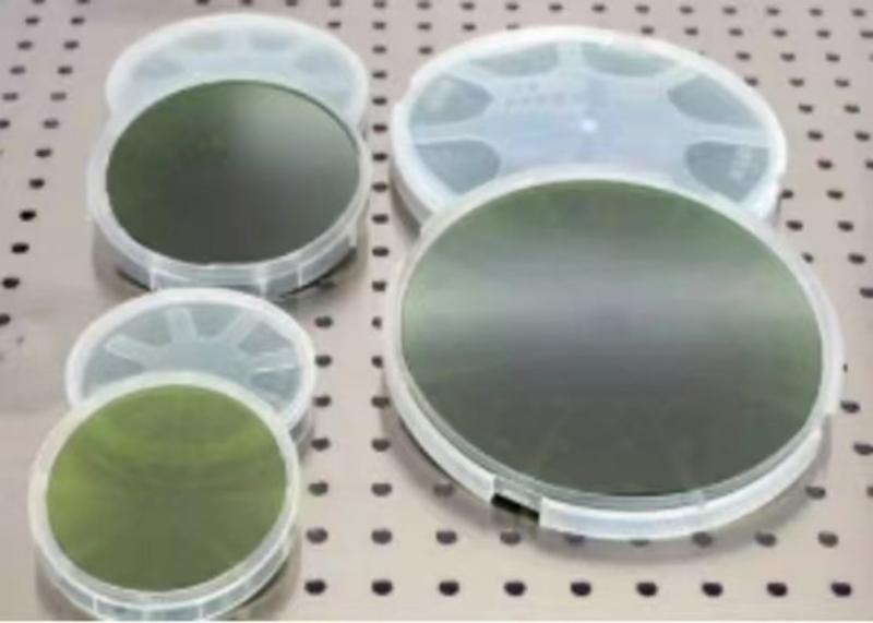
The silicon carbide substrate is divided into semi-insulating type and conductive type. At present, the mainstream specification of semi-insulated silicon carbide substrate products is 4 inches. In the conductive silicon carbide market, the current mainstream substrate product specification is 6 inches.
Due to downstream applications in the RF field, semi-insulated SiC substrates and epitaxial materials are subject to export control by the US Department of Commerce. Semi-insulated SiC as substrate is the preferred material for GaN heteroepitaxy and has important application prospects in microwave field. Compared with the crystal mismatch of sapphire 14% and Si 16.9%, the crystal mismatch of SiC and GaN materials is only 3.4%. Coupled with the ultra-high thermal conductivity of SiC, The high energy efficiency LED and GaN high frequency and high power microwave devices prepared by it have great advantages in radar, high power microwave equipment and 5G communication systems.
The research and development of semi-insulated SiC substrate has always been the focus of the research and development of SiC single crystal substrate. There are two main difficulties in growing semi-insulated SiC materials:
1) Reduce the N donor impurities introduced by graphite crucible, thermal insulation adsorption and doping in powder;
2) While ensuring the quality and electrical properties of the crystal, a deep level center is introduced to compensate the residual shallow level impurities with electrical activity.
At present, the manufacturers with semi-insulated SiC production capacity are mainly SICC Co,Semisic Crystal Co,Tanke Blue Co, Hebei Synlight Crystal Co., Ltd.
The conductive SiC crystal is achieved by injecting nitrogen into the growing atmosphere. Conductive silicon carbide substrate is mainly used in the manufacture of power devices, silicon carbide power devices with high voltage, high current, high temperature, high frequency, low loss and other unique advantages, will greatly improve the existing use of silicon based power devices energy conversion efficiency, has a significant and far-reaching impact on the field of efficient energy conversion. The main application areas are electric vehicles/charging piles, photovoltaic new energy, rail transit, smart grid and so on. Because the downstream of conductive products are mainly power devices in electric vehicles, photovoltaic and other fields, the application prospect is broader, and the manufacturers are more numerous.
Silicon carbide crystal type: The typical structure of the best 4H crystalline silicon carbide can be divided into two categories, one is the cubic silicon carbide crystal type of sphalerite structure, known as 3C-SiC or β-SiC, and the other is the hexagonal or diamond structure of the large period structure, which is typical of 6H-SiC, 4H-sic, 15R-SiC, etc., collectively known as α-SiC. 3C-SiC has the advantage of high resistivity in manufacturing devices. However, the high mismatch between Si and SiC lattice constants and thermal expansion coefficients can lead to a large number of defects in the 3C-SiC epitaxial layer. 4H-SiC has great potential in manufacturing MOSFETs, because its crystal growth and epitaxial layer growth processes are more excellent, and in terms of electron mobility, 4H-SiC is higher than 3C-SiC and 6H-SiC, providing better microwave characteristics for 4H-SiC MOSFETs.
If there is infringement, contact delete
Post time: Jul-16-2024