SOI (Silicon-On-Insulator) wafers represent a specialized semiconductor material featuring an ultra-thin silicon layer formed atop an insulating oxide layer. This unique sandwich structure delivers significant performance enhancements for semiconductor devices.
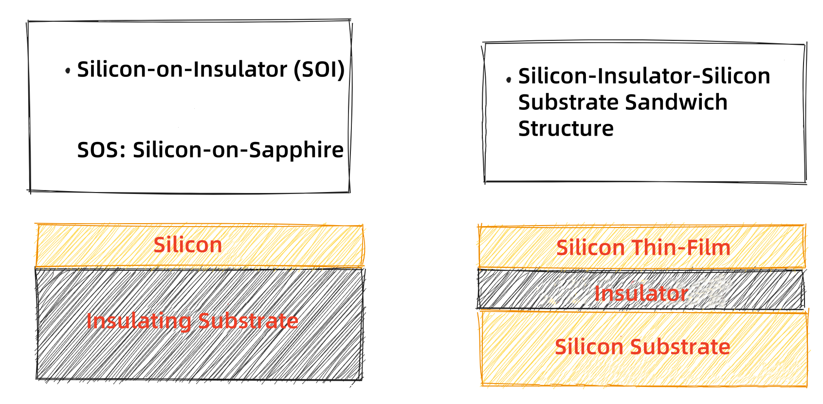
Structural Composition:
Device Layer (Top Silicon):
Thickness ranging from several nanometers to micrometers, serving as the active layer for transistor fabrication.
Buried Oxide Layer (BOX):
A silicon dioxide insulating layer (0.05-15μm thick) that electrically isolates the device layer from the substrate.
Base Substrate:
Bulk silicon (100-500μm thick) providing mechanical support.
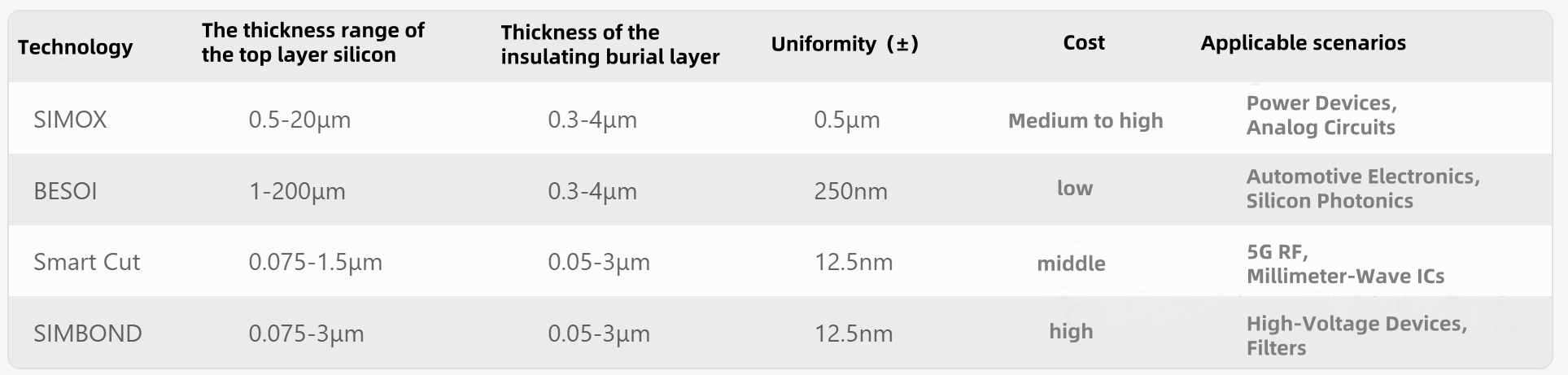
According to the preparation process technology, the mainstream process routes of SOI silicon wafers can be classified as: SIMOX (oxygen injection isolation technology), BESOI (bonding thinning technology), and Smart Cut (intelligent stripping technology).
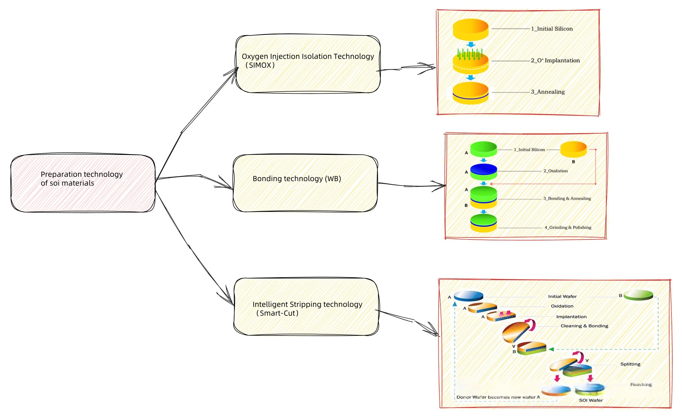
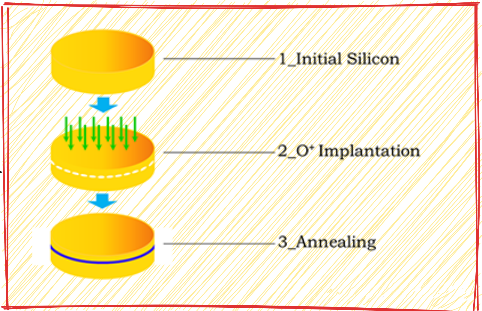
SIMOX (Oxygen injection isolation technology) is a technique that involves injecting high-energy oxygen ions into silicon wafers to form a silicon dioxide embedded layer, which is then subjected to high-temperature annealing to repair lattice defects. The core is direct ion oxygen injection to form buried layer oxygen.
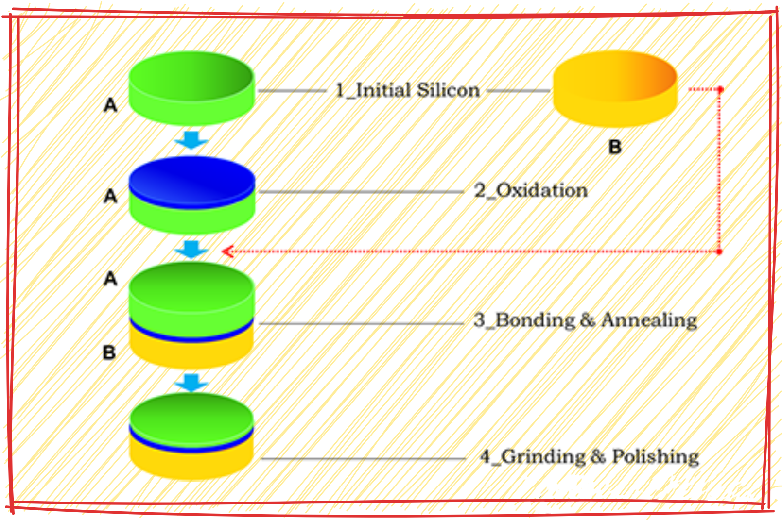
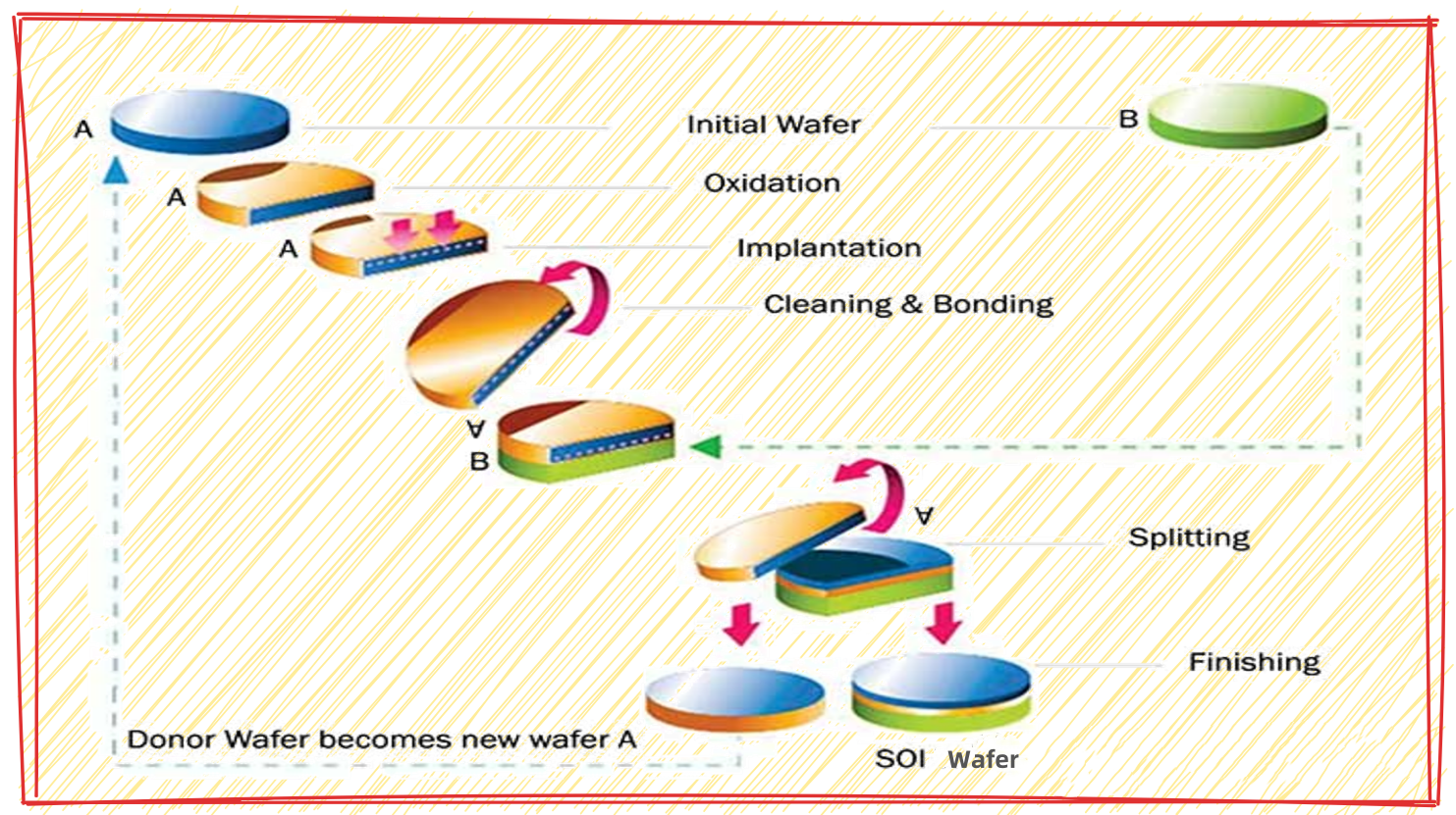
BESOI (Bonding Thinning technology) involves bonding two silicon wafers and then thinning one of them through mechanical grinding and chemical etching to form an SOI structure. The core lies in bonding and thinning.
Smart Cut (Intelligent Exfoliation technology) forms an exfoliation layer through hydrogen ion injection. After bonding, heat treatment is carried out to exfoliate the silicon wafer along the hydrogen ion layer, forming an ultra-thin silicon layer. The core is hydrogen injection stripping.
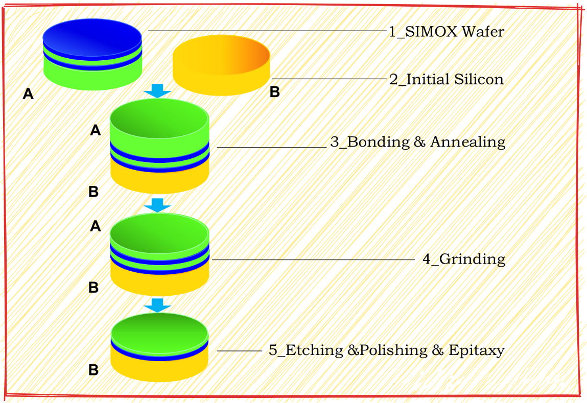
Currently, there is another technology known as SIMBOND (oxygen injection bonding technology), which was developed by Xinao. In fact, it is a route that combines oxygen injection isolation and bonding technologies. In this technical route, the injected oxygen is used as a thinning barrier layer, and the actual buried oxygen layer is a thermal oxidation layer. Therefore, it simultaneously improves parameters such as the uniformity of the top silicon and the quality of the buried oxygen layer.
SOI silicon wafers manufactured by different technical routes have different performance parameters and are suitable for different application scenarios.
The following is a summary table of the core performance advantages of SOI silicon wafers, combined with their technical features and actual application scenarios. Compared with traditional bulk silicon, SOI has significant advantages in the balance of speed and power consumption. (PS: The performance of 22nm FD-SOI is close to that of FinFET, and the cost is reduced by 30%.)
| Performance Advantage | Technical Principle | Specific Manifestation | Typical Application Scenarios |
| Low Parasitic Capacitance | Insulating layer (BOX) blocks charge coupling between device and substrate | Switching speed increased by 15%-30%, power consumption reduced by 20%-50% | 5G RF, High-frequency communication chips |
| Reduced Leakage Current | Insulating layer suppresses leakage current paths | Leakage current reduced by >90%, extended battery life | IoT devices, Wearable electronics |
| Enhanced Radiation Hardness | Insulating layer blocks radiation-induced charge accumulation | Radiation tolerance improved 3-5x, reduced single-event upsets | Spacecraft, Nuclear industry equipment |
| Short-Channel Effect Control | Thin silicon layer reduces electric field interference between drain and source | Improved threshold voltage stability, optimized subthreshold slope | Advanced node logic chips (<14nm) |
| Improved Thermal Management | Insulating layer reduces thermal conduction coupling | 30% less heat accumulation, 15-25°C lower operating temperature | 3D ICs, Automotive electronics |
| High-Frequency Optimization | Reduced parasitic capacitance and enhanced carrier mobility | 20% lower delay, supports >30GHz signal processing | mmWave communication, Satellite comm chips |
| Increased Design Flexibility | No well doping required, supports back biasing | 13%-20% fewer process steps, 40% higher integration density | Mixed-signal ICs, Sensors |
| Latch-up Immunity | Insulating layer isolates parasitic PN junctions | Latch-up current threshold increased to >100mA | High-voltage power devices |
To sum up, the main advantages of SOI are: it runs fast and is more power-efficient.
Due to these performance characteristics of SOI, it has wide applications in fields that require excellent frequency performance and power consumption performance.
As shown below, based on the proportion of application fields corresponding to SOI, it can be seen that RF and power devices account for the vast majority of the SOI market.
| Application Field | Market Share |
| RF-SOI (Radio Frequency) | 45% |
| Power SOI | 30% |
| FD-SOI (Fully Depleted) | 15% |
| Optical SOI | 8% |
| Sensor SOI | 2% |
With the growth of markets such as mobile communication and autonomous driving, SOI silicon wafers are also expected to maintain a certain growth rate.
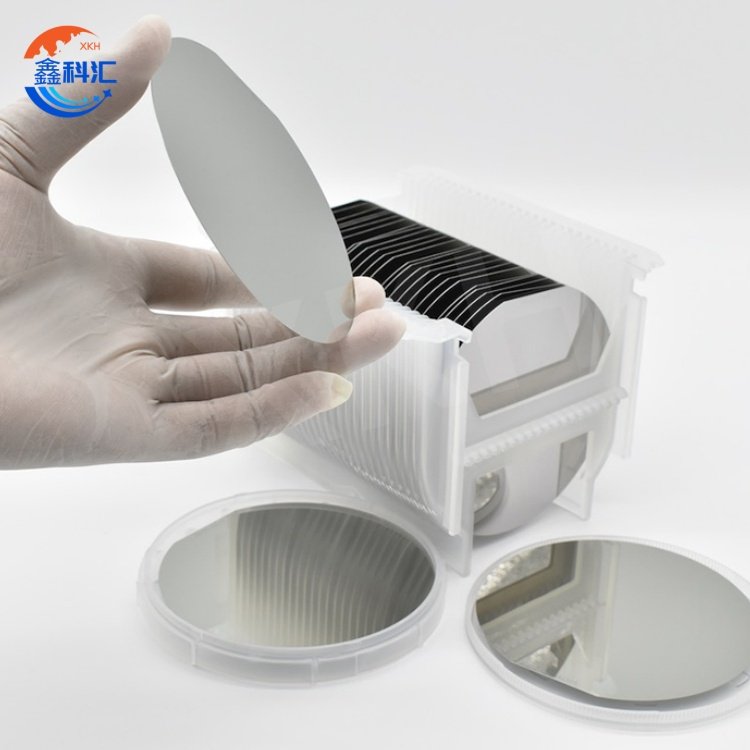
XKH, as a leading innovator in Silicon-On-Insulator (SOI) wafer technology, delivers comprehensive SOI solutions from R&D to volume production utilizing industry-leading manufacturing processes. Our complete portfolio includes 200mm/300mm SOI wafers spanning RF-SOI, Power-SOI and FD-SOI variants, with stringent quality control ensuring exceptional performance consistency (thickness uniformity within ±1.5%). We offer customized solutions with buried oxide (BOX) layer thickness ranging from 50nm to 1.5μm and various resistivity specifications to meet specific requirements. Leveraging 15 years of technical expertise and a robust global supply chain, we reliably provide high-quality SOI substrate materials to top-tier semiconductor manufacturers worldwide, enabling cutting-edge chip innovations in 5G communications, automotive electronics, and artificial intelligence applications.
XKH’s SOI wafers:
Post time: Apr-24-2025