Crystal planes and crystal orientation are two core concepts in crystallography, closely related to the crystal structure in silicon-based integrated circuit technology.
1.Definition and Properties of Crystal Orientation
Crystal orientation represents a specific direction within a crystal, typically expressed by crystal orientation indices. Crystal orientation is defined by connecting any two lattice points within the crystal structure, and it has the following characteristics: each crystal orientation contains an infinite number of lattice points; a single crystal orientation can consist of multiple parallel crystal orientations forming a crystal orientation family; the crystal orientation family covers all lattice points within the crystal.
The significance of crystal orientation lies in indicating the directional arrangement of atoms within the crystal. For example, the [111] crystal orientation represents a specific direction where the projection ratios of the three coordinate axes are 1:1:1.
2. Definition and Properties of Crystal Planes
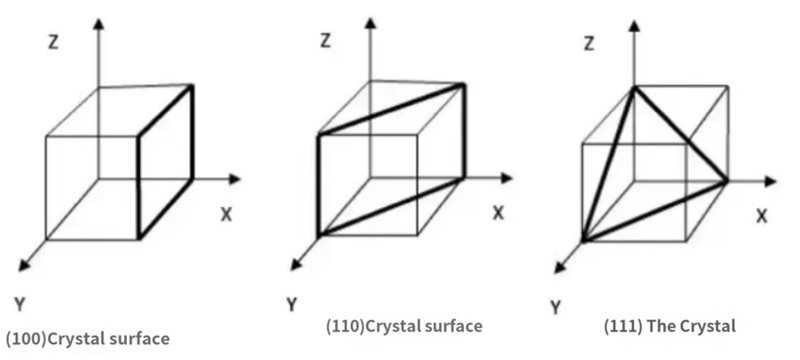
A crystal plane is a plane of atom arrangement within a crystal, represented by crystal plane indices (Miller indices). For example, (111) indicates that the reciprocals of the intercepts of the crystal plane on the coordinate axes are in the ratio of 1:1:1. The crystal plane has the following properties: each crystal plane contains an infinite number of lattice points; each crystal plane has an infinite number of parallel planes forming a crystal plane family; the crystal plane family covers the entire crystal.
The determination of Miller indices involves taking the intercepts of the crystal plane on each coordinate axis, finding their reciprocals, and converting them into the smallest integer ratio. For example, the (111) crystal plane has intercepts on the x, y, and z axes in the ratio of 1:1:1.
3. The Relationship Between Crystal Planes and Crystal Orientation
Crystal planes and crystal orientation are two different ways of describing the geometric structure of a crystal. Crystal orientation refers to the arrangement of atoms along a specific direction, while a crystal plane refers to the arrangement of atoms on a specific plane. These two have a certain correspondence, but they represent different physical concepts.
Key relationship: The normal vector of a crystal plane (i.e., the vector perpendicular to that plane) corresponds to a crystal orientation. For example, the normal vector of the (111) crystal plane corresponds to the [111] crystal orientation, meaning that the atomic arrangement along the [111] direction is perpendicular to that plane.
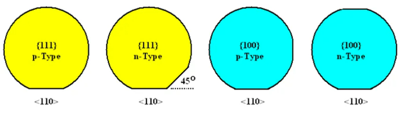
In semiconductor processes, the selection of crystal planes greatly affects device performance. For example, in silicon-based semiconductors, commonly used crystal planes are the (100) and (111) planes because they have different atomic arrangements and bonding methods in different directions. Properties such as electron mobility and surface energy vary on different crystal planes, influencing the performance and growth process of semiconductor devices.
4. Practical Applications in Semiconductor Processes
In silicon-based semiconductor manufacturing, crystal orientation and crystal planes are applied in many aspects:
Crystal Growth: Semiconductor crystals are typically grown along specific crystal orientations. Silicon crystals most commonly grow along the [100] or [111] orientations because the stability and atomic arrangement in these orientations are favorable for crystal growth.
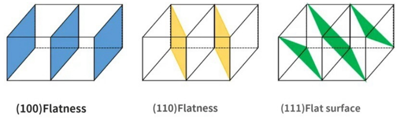
Etching Process: In wet etching, different crystal planes have varying etching rates. For example, the etching rates on the (100) and (111) planes of silicon differ, resulting in anisotropic etching effects.
Device Characteristics: The electron mobility in MOSFET devices is affected by the crystal plane. Typically, the mobility is higher on the (100) plane, which is why modern silicon-based MOSFETs predominantly use (100) wafers.
In summary, crystal planes and crystal orientations are two fundamental ways to describe the structure of crystals in crystallography. Crystal orientation represents the directional properties within a crystal, while crystal planes describe specific planes within the crystal. These two concepts are closely related in semiconductor manufacturing. The selection of crystal planes directly impacts the material’s physical and chemical properties, while crystal orientation influences crystal growth and processing techniques. Understanding the relationship between crystal planes and orientations is crucial for optimizing semiconductor processes and improving device performance.
Post time: Oct-08-2024