In the booming development process of the semiconductor industry, polished single crystal silicon wafers play a crucial role. They serve as the fundamental material for the production of various microelectronic devices. From complex and precise integrated circuits to high-speed microprocessors and multifunctional sensors, polished single crystal silicon wafers are essential. The differences in their performance and specifications directly impact the quality and performance of the final products. Below are the common specifications and parameters of polished single crystal silicon wafers:
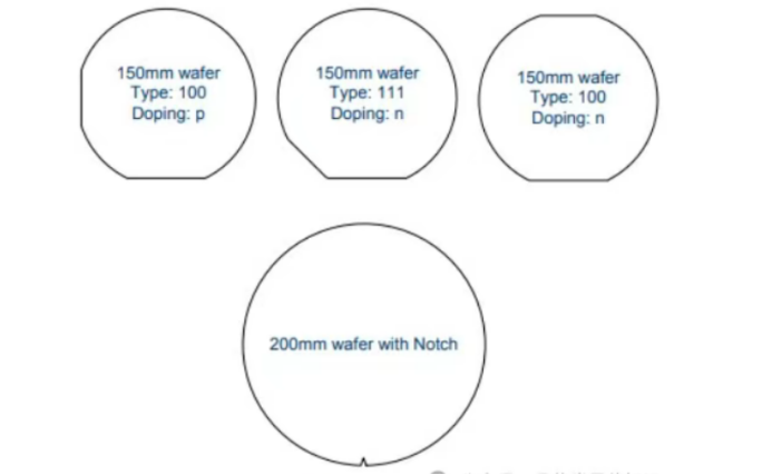
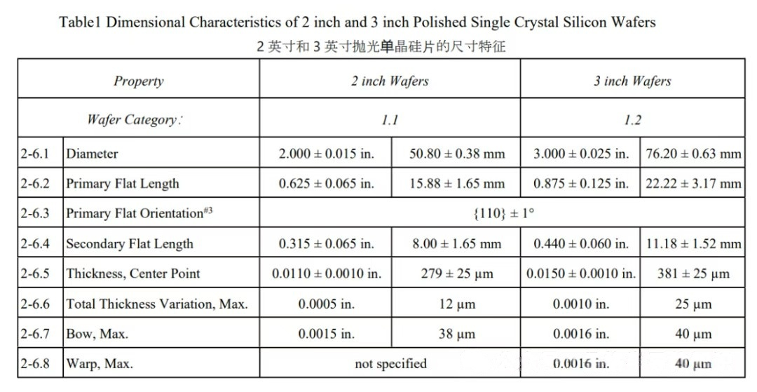
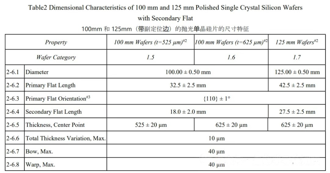
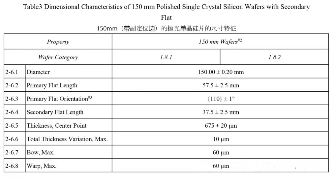
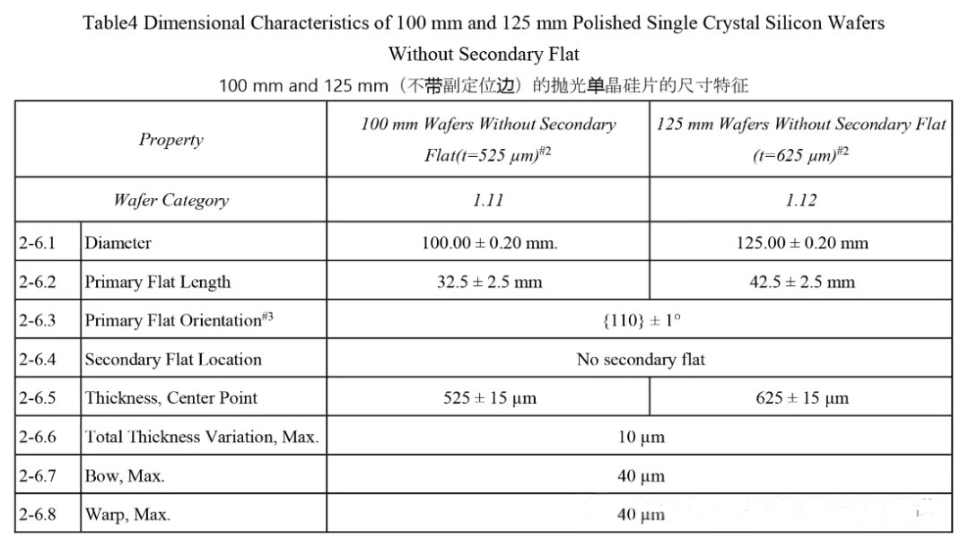
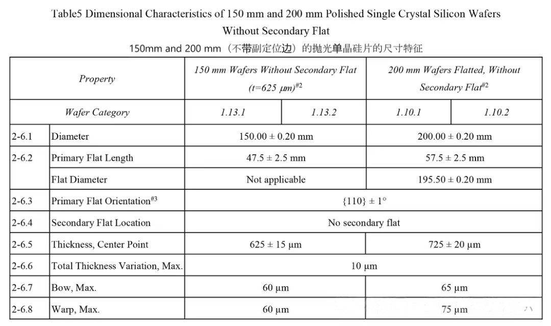
Diameter: The size of semiconductor single crystal silicon wafers is measured by their diameter, and they come in a variety of specifications. Common diameters include 2 inches (50.8mm), 3 inches (76.2mm), 4 inches (100mm), 5 inches (125mm), 6 inches (150mm), 8 inches (200mm), 12 inches (300mm), and 18 inches (450mm). Different diameters are suited for various production needs and process requirements. For example, smaller diameter wafers are commonly used for special, small-volume microelectronic devices, while larger diameter wafers demonstrate higher production efficiency and cost advantages in large-scale integrated circuit manufacturing. Surface requirements are categorized as single-side polished (SSP) and double-side polished (DSP). Single-side polished wafers are used for devices requiring high flatness on one side, such as certain sensors. Double-side polished wafers are commonly used for integrated circuits and other products that require high precision on both surfaces. Surface Requirement (Finish): Single-side polished SSP / Double-side polished DSP.
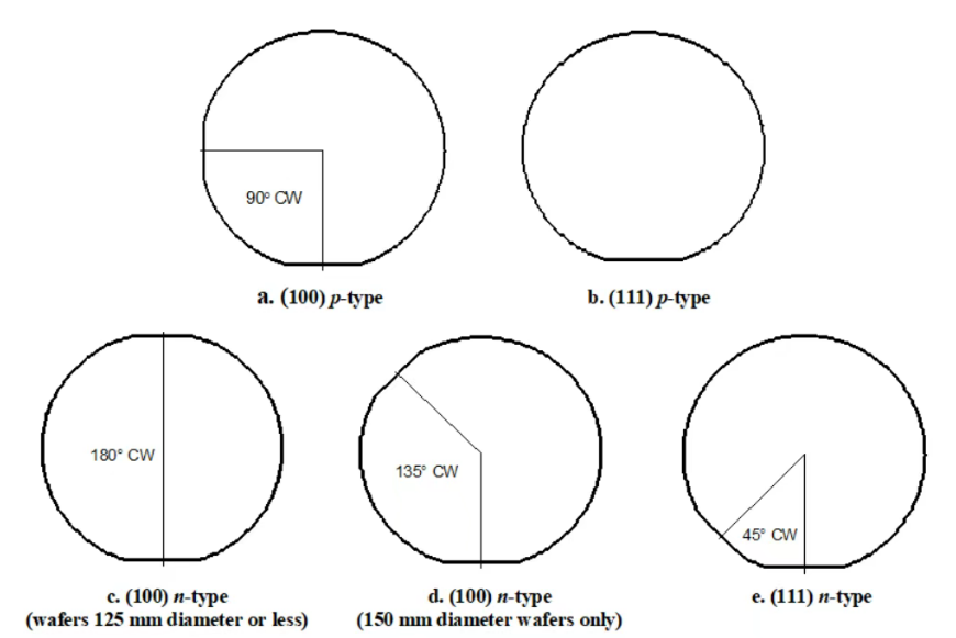
Type/Dopant: (1) N-type Semiconductor: When certain impurity atoms are introduced into the intrinsic semiconductor, they alter its conductivity. For example, when pentavalent elements like nitrogen (N), phosphorus (P), arsenic (As), or antimony (Sb) are added, their valence electrons form covalent bonds with the valence electrons of the surrounding silicon atoms, leaving an extra electron not bound by a covalent bond. This results in an electron concentration greater than the hole concentration, forming an N-type semiconductor, also known as an electron-type semiconductor. N-type semiconductors are crucial in manufacturing devices that require electrons as the main charge carriers, such as certain power devices. (2) P-type Semiconductor: When trivalent impurity elements like boron (B), gallium (Ga), or indium (In) are introduced into the silicon semiconductor, the valence electrons of the impurity atoms form covalent bonds with the surrounding silicon atoms, but they lack at least one valence electron and cannot form a complete covalent bond. This leads to a hole concentration greater than the electron concentration, forming a P-type semiconductor, also known as a hole-type semiconductor. P-type semiconductors play a key role in manufacturing devices where holes serve as the main charge carriers, such as diodes and certain transistors.
Resistivity: Resistivity is a key physical quantity that measures the electrical conductivity of polished single crystal silicon wafers. Its value reflects the material’s conductive performance. The lower the resistivity, the better the conductivity of the silicon wafer; conversely, the higher the resistivity, the poorer the conductivity. The resistivity of silicon wafers is determined by their inherent material properties, and temperature has a significant impact as well. Generally, the resistivity of silicon wafers increases with temperature. In practical applications, different microelectronic devices have different resistivity requirements for silicon wafers. For example, wafers used in integrated circuit manufacturing need precise control of resistivity to ensure stable and reliable device performance.
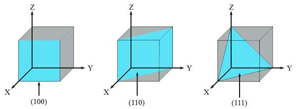
Orientation: The crystal orientation of the wafer represents the crystallographic direction of the silicon lattice, typically specified by Miller indices such as (100), (110), (111), etc. Different crystal orientations have different physical properties, such as line density, which varies based on the orientation. This difference can affect the wafer’s performance in subsequent processing steps and the final performance of microelectronic devices. In the manufacturing process, selecting a silicon wafer with the appropriate orientation for different device requirements can optimize device performance, improve production efficiency, and enhance product quality.
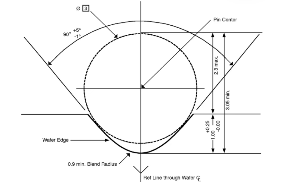
Flat/Notch: The flat edge (Flat) or V-notch (Notch) on the circumference of the silicon wafer plays a critical role in crystal orientation alignment and is an important identifier in the manufacturing and processing of the wafer. Wafers of different diameters correspond to different standards for the length of the Flat or Notch. The alignment edges are classified into primary flat and secondary flat. The primary flat is mainly used to determine the basic crystal orientation and processing reference of the wafer, while the secondary flat further assists in precise alignment and processing, ensuring accurate operation and consistency of the wafer throughout the production line.
Thickness: The thickness of a wafer is typically specified in micrometers (μm), with common thickness ranges between 100μm and 1000μm. Wafers of different thicknesses are suitable for different types of microelectronic devices. Thinner wafers (e.g., 100μm – 300μm) are often used for chip manufacturing that requires strict thickness control, reducing the size and weight of the chip and increasing the integration density. Thicker wafers (e.g., 500μm – 1000μm) are widely used in devices that require higher mechanical strength, such as power semiconductor devices, to ensure stability during operation.
Surface Roughness: Surface roughness is one of the key parameters for evaluating wafer quality, as it directly affects the adhesion between the wafer and subsequent deposited thin film materials, as well as the electrical performance of the device. It is usually expressed as the root mean square (RMS) roughness (in nm). Lower surface roughness means the wafer surface is smoother, which helps reduce phenomena like electron scattering and improves device performance and reliability. In advanced semiconductor manufacturing processes, surface roughness requirements are becoming increasingly stringent, especially for high-end integrated circuit manufacturing, where surface roughness must be controlled to a few nanometers or even lower.
Total Thickness Variation (TTV): Total thickness variation refers to the difference between the maximum and minimum thicknesses measured at multiple points on the wafer surface, typically expressed in μm. A high TTV may lead to deviations in processes such as photolithography and etching, impacting device performance consistency and yield. Therefore, controlling TTV during wafer manufacturing is a key step in ensuring product quality. For high-precision microelectronic device manufacturing, TTV is typically required to be within a few micrometers.
Bow: Bow refers to the deviation between the wafer surface and the ideal flat plane, typically measured in μm. Wafers with excessive bowing may break or experience uneven stress during subsequent processing, affecting production efficiency and product quality. Especially in processes that require high flatness, such as photolithography, bowing must be controlled within a specific range to ensure the accuracy and consistency of the photolithographic pattern.
Warp: Warp indicates the deviation between the wafer surface and the ideal spherical shape, also measured in μm. Similar to bow, warp is an important indicator of wafer flatness. Excessive warp not only affects the placement accuracy of the wafer in processing equipment but can also cause issues during the chip packaging process, such as poor bonding between the chip and packaging material, which in turn affects the reliability of the device. In high-end semiconductor manufacturing, warp requirements are becoming more stringent to meet the demands of advanced chip manufacturing and packaging processes.
Edge Profile: The edge profile of a wafer is critical for its subsequent processing and handling. It is typically specified by the Edge Exclusion Zone (EEZ), which defines the distance from the wafer edge where no processing is allowed. A properly designed edge profile and precise EEZ control help avoid edge defects, stress concentrations, and other issues during processing, improving the overall wafer quality and yield. In some advanced manufacturing processes, edge profile precision is required to be at the sub-micron level.
Particle Count: The number and size distribution of particles on the wafer surface significantly affect the performance of microelectronic devices. Excessive or large particles may lead to device failures, such as short circuits or leakage, reducing product yield. Therefore, particle count is usually measured by counting the particles per unit area, such as the number of particles larger than 0.3μm. Strict control of particle count during wafer manufacturing is an essential measure for ensuring product quality. Advanced cleaning technologies and a clean production environment are used to minimize particle contamination on the wafer surface.
Related production
Single Crystal Silicon Wafer Si Substrate Type N/P Optional Silicon Carbide Wafer
FZ CZ Si wafer in stock 12inch Silicon wafer Prime or Test
Post time: Apr-18-2025