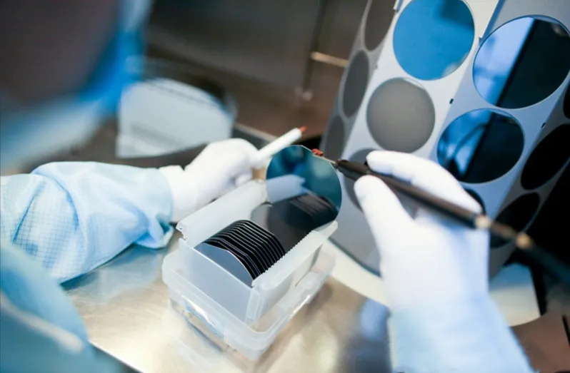
In daily life, electronic devices such as smartphones and smartwatches have become indispensable companions. These devices are becoming increasingly slim yet more powerful. Have you ever wondered what enables their continuous evolution? The answer lies in semiconductor materials, and today, we focus on one of the most outstanding among them—sapphire crystal.
Sapphire crystal, primarily composed of α-Al₂O₃, consists of three oxygen atoms and two aluminum atoms bonded covalently, forming a hexagonal lattice structure. While it resembles gem-grade sapphire in appearance, industrial sapphire crystals emphasize superior performance. Chemically inert, it is insoluble in water and resistant to acids and alkalis, acting as a “chemical shield” that maintains stability in harsh environments. Additionally, it exhibits excellent optical transparency, allowing efficient light transmission; strong thermal conductivity, preventing overheating; and outstanding electrical insulation, ensuring stable signal transmission without leakage. Mechanically, sapphire boasts a Mohs hardness of 9, second only to diamond, making it highly wear- and erosion-resistant—ideal for demanding applications.
The Secret Weapon in Chip Manufacturing
(1) Key Material for Low-Power Chips
As electronics trend toward miniaturization and high performance, low-power chips have become critical. Traditional chips suffer from insulation degradation at nanoscale thicknesses, leading to current leakage, increased power consumption, and overheating, which compromises stability and lifespan.
Researchers at the Shanghai Institute of Microsystem and Information Technology (SIMIT), Chinese Academy of Sciences, developed artificial sapphire dielectric wafers using metal-intercalated oxidation technology, converting single-crystal aluminum into single-crystal alumina (sapphire). At 1 nm thickness, this material exhibits ultra-low leakage current, outperforming conventional amorphous dielectrics by two orders of magnitude in state density reduction and improving interface quality with 2D semiconductors. Integrating this with 2D materials enables low-power chips, significantly extending battery life in smartphones and enhancing stability in AI and IoT applications.
(2) The Perfect Partner for Gallium Nitride (GaN)
In the semiconductor field, gallium nitride (GaN) has emerged as a shining star due to its unique advantages. As a wide-bandgap semiconductor material with a bandgap of 3.4 eV—significantly larger than silicon’s 1.1 eV—GaN excels in high-temperature, high-voltage, and high-frequency applications. Its high electron mobility and critical breakdown field strength make it an ideal material for high-power, high-temperature, high-frequency, and high-brightness electronic devices. In power electronics, GaN-based devices operate at higher frequencies with lower energy consumption, offering superior performance in power conversion and energy management. In microwave communications, GaN enables high-power, high-frequency components such as 5G power amplifiers, enhancing signal transmission quality and stability.
Sapphire crystal is considered the “perfect partner” for GaN. Although its lattice mismatch with GaN is higher than that of silicon carbide (SiC), sapphire substrates exhibit lower thermal mismatch during GaN epitaxy, providing a stable foundation for GaN growth. Additionally, sapphire’s excellent thermal conductivity and optical transparency facilitate efficient heat dissipation in high-power GaN devices, ensuring operational stability and optimal light output efficiency. Its superior electrical insulation properties further minimize signal interference and power loss. The combination of sapphire and GaN has led to the development of high-performance devices, including GaN-based LEDs, which dominate the lighting and display markets—from household LED bulbs to large outdoor screens—as well as laser diodes used in optical communications and precision laser processing.
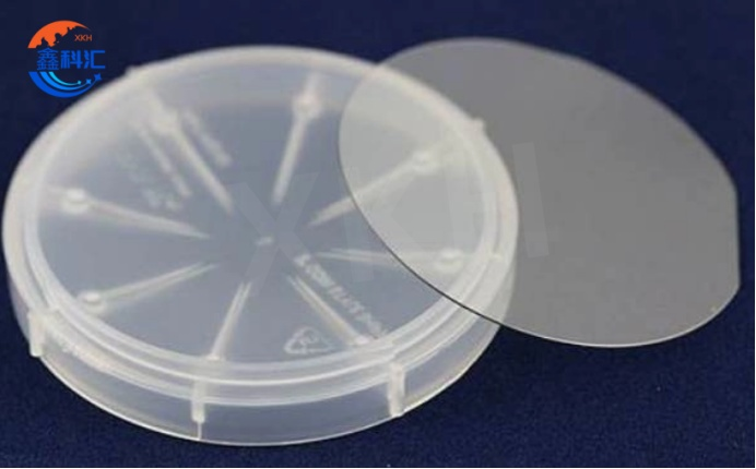
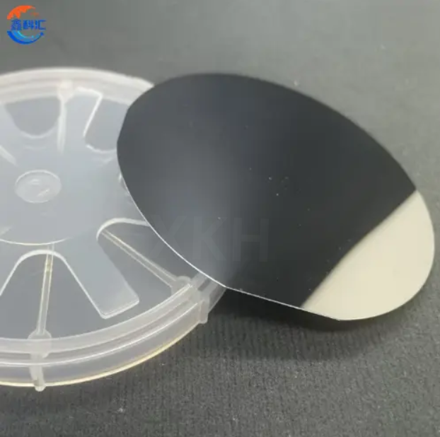
XKH’s GaN-on-sapphire wafer
Expanding the Boundaries of Semiconductor Applications
(1) The “Shield” in Military and Aerospace Applications
Equipment in military and aerospace applications often operates under extreme conditions. In space, spacecraft endure near-absolute-zero temperatures, intense cosmic radiation, and the challenges of a vacuum environment. Military aircraft, meanwhile, face surface temperatures exceeding 1,000°C due to aerodynamic heating during high-speed flight, along with high mechanical loads and electromagnetic interference.
Sapphire crystal’s unique properties make it an ideal material for critical components in these fields. Its exceptional high-temperature resistance—withstanding up to 2,045°C while maintaining structural integrity—ensures reliable performance under thermal stress. Its radiation hardness also preserves functionality in cosmic and nuclear environments, effectively shielding sensitive electronics. These attributes have led to sapphire’s widespread use in high-temperature infrared (IR) windows. In missile guidance systems, IR windows must maintain optical clarity under extreme heat and velocity to ensure accurate target detection. Sapphire-based IR windows combine high thermal stability with superior IR transmittance, significantly improving guidance precision. In aerospace, sapphire protects satellite optical systems, enabling clear imaging in harsh orbital conditions.
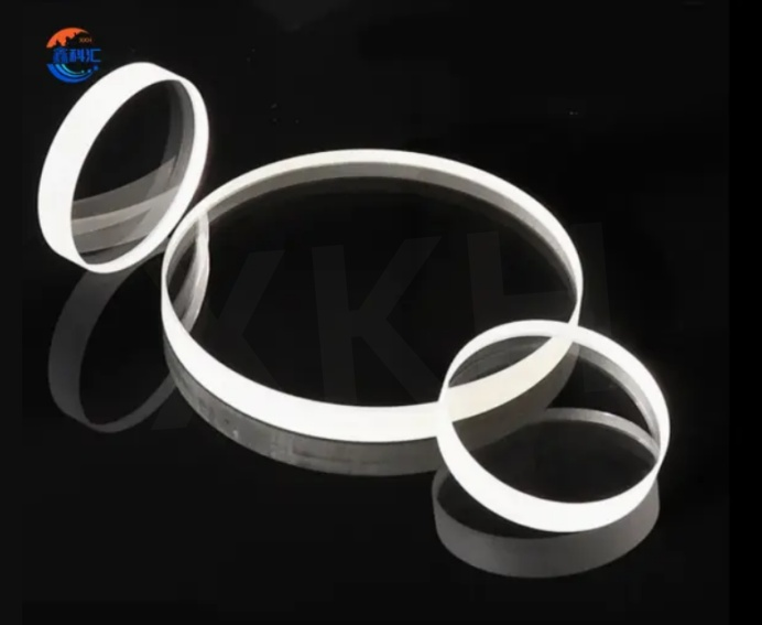
XKH’s sapphire optical windows
(2) The New Foundation for Superconductors and Microelectronics
In superconductivity, sapphire serves as an indispensable substrate for superconducting thin films, which enable zero-resistance conduction—revolutionizing power transmission, maglev trains, and MRI systems. High-performance superconducting films require substrates with stable lattice structures, and sapphire’s compatibility with materials like magnesium diboride (MgB₂) allows the growth of films with enhanced critical current density and critical magnetic field. For example, power cables using sapphire-supported superconducting films dramatically improve transmission efficiency by minimizing energy loss.
In microelectronics, sapphire substrates with specific crystallographic orientations—such as R-plane (<1-102>) and A-plane (<11-20>)—enable tailored silicon epitaxial layers for advanced integrated circuits (ICs). R-plane sapphire reduces crystal defects in high-speed ICs, boosting operational speed and stability, while A-plane sapphire’s insulating properties and uniform permittivity optimize hybrid microelectronics and high-temperature superconductor integration. These substrates underpin core chips in high-performance computing and telecommunications infrastructure.
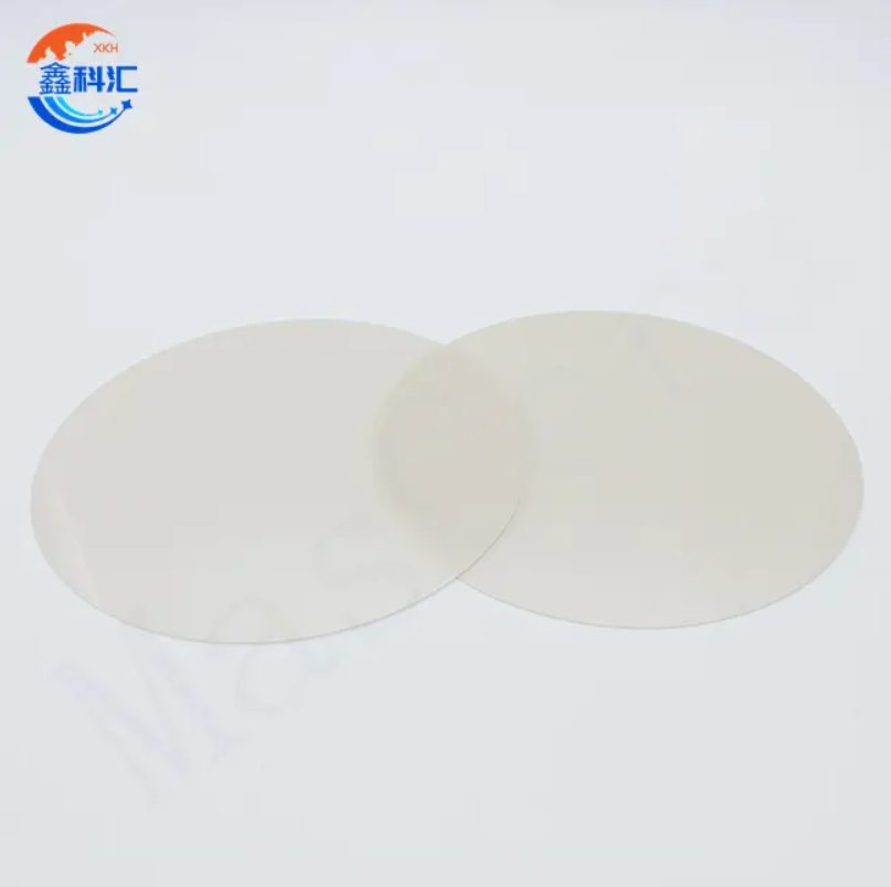
XKH‘s AlN-on-NPSS Wafer
The Future of Sapphire Crystal in Semiconductors
Sapphire has already demonstrated immense value across semiconductors, from chip fabrication to aerospace and superconductors. As technology advances, its role will expand further. In artificial intelligence, sapphire-supported low-power, high-performance chips will drive AI advancements in healthcare, transportation, and finance. In quantum computing, sapphire’s material properties position it as a promising candidate for qubit integration. Meanwhile, GaN-on-sapphire devices will meet escalating demands for 5G/6G communication hardware. Moving forward, sapphire will remain a cornerstone of semiconductor innovation, powering humanity’s technological progress.
XKH’s GaN-on-sapphire epitaxial wafer
XKH delivers precision-engineered sapphire optical windows and GaN-on-sapphire wafer solutions for cutting-edge applications. Leveraging proprietary crystal growth and nanoscale polishing technologies, we provide ultra-flat sapphire windows with exceptional transmission from UV to IR spectra, ideal for aerospace, defense, and high-power laser systems.
Post time: Apr-18-2025