With the continuous development of semiconductor technology, in the semiconductor industry and even the photovoltaic industry, the requirements for the surface quality of the wafer substrate or epitaxial sheet are also very strict. So, what are the quality requirements for wafers? Taking sapphire wafers as an example, what indicators can be used to evaluate the surface quality of wafers?

What are the wafers evaluation indicators?
The Three indicators
For sapphire wafers, its evaluation indicators are total thickness deviation (TTV), bend (Bow) and Warp (Warp). These three parameters together reflect the flatness and thickness uniformity of the silicon wafer, and can measure the degree of ripple of the wafer. The corrugation can be combined with the flatness to evaluate the quality of the wafer surface.
What is TTV, BOW, Warp?
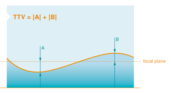
TTV (Total Thickness Variation)

TTV is the difference between the maximum and minimum thickness of a wafer. This parameter is an important index used to measure wafer thickness uniformity. In a semiconductor process, the thickness of the wafer must be very uniform over the entire surface. Measurements are usually made at five locations on the wafer and the difference is calculated. Ultimately, this value is an important basis for judging the quality of the wafer.
Bow

Bow in semiconductor manufacturing refers to the bend of a wafer, freeing the distance between the midpoint of an unclamped wafer and the reference plane. The word probably comes from a description of the shape of an object when it is bent, like the curved shape of a bow. The Bow value is defined by measuring the deviation between the center and edge of the silicon wafer. This value is usually expressed in micrometers (µm).
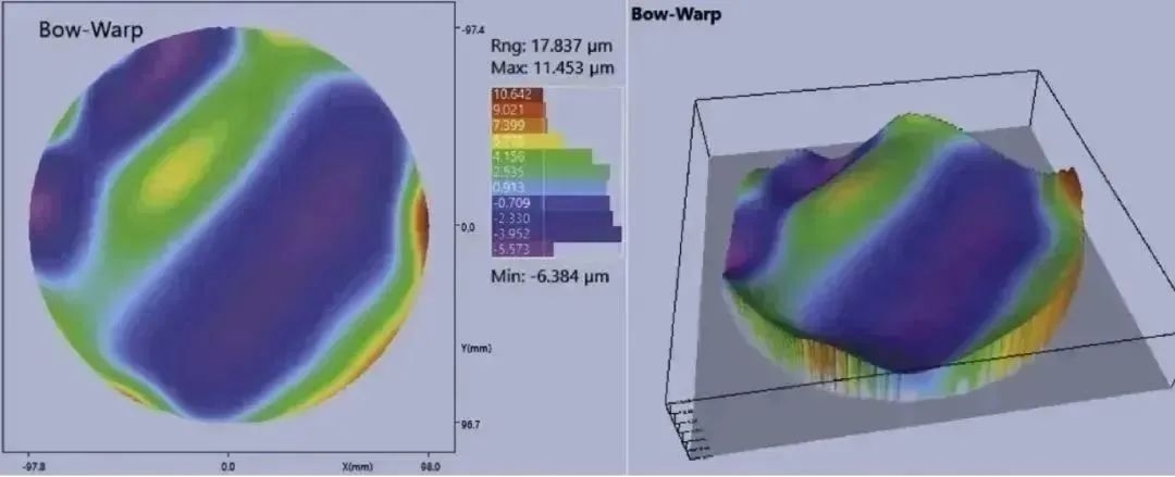
Warp
Warp is a global property of wafers that measures the difference between the maximum and minimum distance between the middle of a freely unclamped wafer and the reference plane. Represents the distance from the surface of the silicon wafer to the plane.
What's the difference between TTV, Bow, Warp?
TTV focuses on changes in thickness and is not concerned with the bending or distortion of the wafer.
Bow focuses on the overall bend, mainly considering the bend of the center point and the edge.
Warp is more comprehensive, including bending and twisting of the entire wafer surface.
Although these three parameters are related to the shape and geometric properties of the silicon wafer, they are measured and described differently, and their impact on the semiconductor process and wafer processing is also different.
The smaller the three parameters, the better, and the larger the parameter, the greater the negative impact on the semiconductor process. Therefore, as a semiconductor practitioner, we must realize the importance of wafer profile parameters for the entire process process, do semiconductor process, must pay attention to details.
(censoring)
Post time: Jun-24-2024