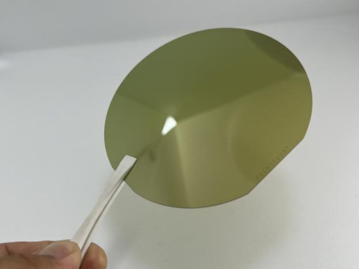
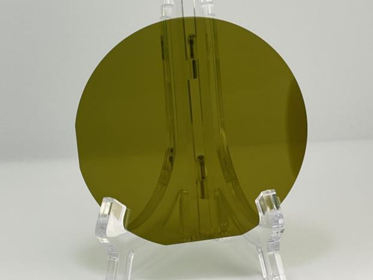
SiC wafers are semiconductors made from silicon carbide. This material was developed in 1893 and is ideal for a variety of applications. Especially suitable for Schottky diodes, junction barrier Schottky diodes, switches and metal-oxide-semiconductor field-effect transistors. Due to its high hardness, it is an excellent choice for power electronic components.
Currently, there are two main types of SiC wafers. The first is a polished wafer, which is a single silicon carbide wafer. It is made of high purity SiC crystals and can be 100mm or 150mm in diameter. It is used in high power electronic devices. The second type is epitaxial crystal silicon carbide wafer. This type of wafer is made by adding a single layer of silicon carbide crystals to the surface. This method requires precise control of the thickness of the material and is known as N-type epitaxy.
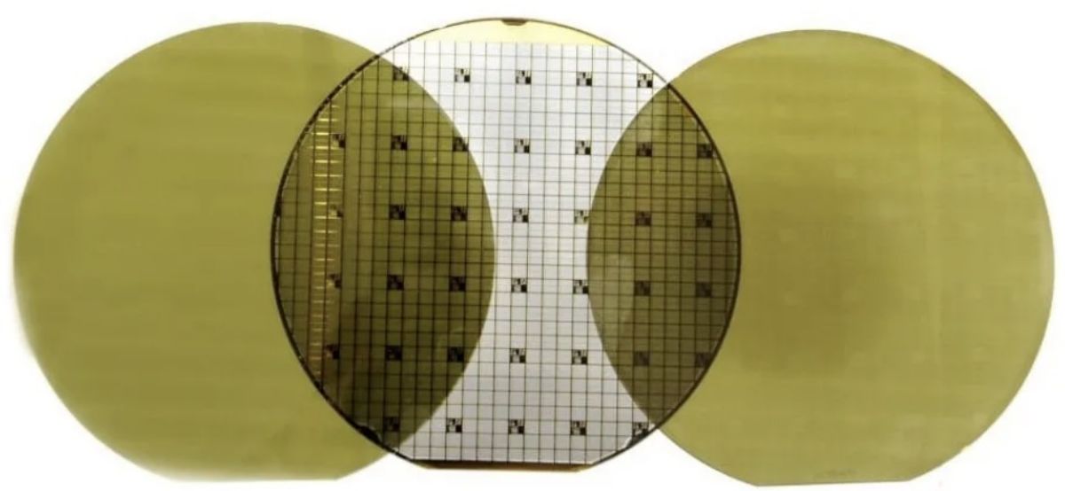
The next type is beta silicon carbide. Beta SiC is produced at temperatures above 1700 degrees Celsius. Alpha carbides are the most common and have a hexagonal crystal structure similar to wurtzite. The beta form is similar to diamond and is used in some applications. It has always been the first choice for electric vehicle power semi-finished products. Several third-party silicon carbide wafer suppliers are currently working on this new material.
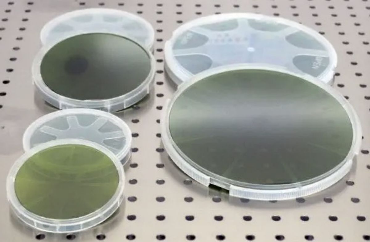
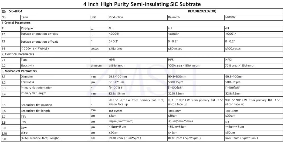
ZMSH SiC wafers are very popular semiconductor materials. It is a high-quality semiconductor material that is well suited for many applications. ZMSH silicon carbide wafers are a very useful material for a variety of electronic devices. ZMSH supplies a wide range of high quality SiC wafers and substrates. They are available in N-type and semi-insulated forms.
2---Silicon Carbide: Towards a new era of wafers
Physical properties and characteristics of silicon carbide
Silicon carbide has a special crystal structure, using a hexagonal close-packed structure similar to diamond. This structure enables silicon carbide to have excellent thermal conductivity and high temperature resistance. Compared to traditional silicon materials, silicon carbide has a larger band gap width, which provides higher electron band spacing, resulting in higher electron mobility and lower leakage current. In addition, silicon carbide also has a higher electron saturation drift speed and a lower resistivity of the material itself, providing better performance for high power applications.

Application cases and prospects of silicon carbide wafers
Power electronics applications
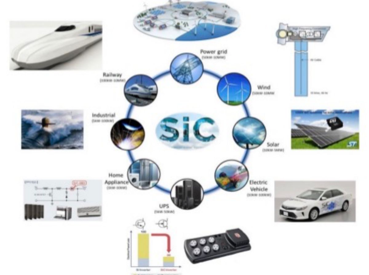
Silicon carbide wafer has wide application prospect in power electronics field. Due to their high electron mobility and excellent thermal conductivity, SIC wafers can be used to manufacture high-power density switching devices, such as power modules for electric vehicles and solar inverters. The high temperature stability of silicon carbide wafers enables these devices to operate in high temperature environments, providing greater efficiency and reliability.
Optoelectronic applications
In the field of optoelectronic devices, silicon carbide wafers show their unique advantages. Silicon carbide material has wide band gap characteristics, which enables it to achieve high photonon energy and low light loss in optoelectronic devices. Silicon carbide wafers can be used to prepare high-speed communication devices, photodetectors and lasers. Its excellent thermal conductivity and low crystal defect density make it ideal for the preparation of high-quality optoelectronic devices.
Outlook
With the growing demand for high-performance electronic devices, silicon carbide wafers have a promising future as a material with excellent properties and wide application potential. With the continuous improvement of preparation technology and the reduction of cost, the commercial application of silicon carbide wafers will be promoted. It is expected that in the next few years, silicon carbide wafers will gradually enter the market and become the mainstream choice for high power, high frequency and high temperature applications.

3---In-depth analysis of SiC wafer market and technology trends
In-depth analysis of silicon carbide (SiC) wafer market drivers
The growth of the silicon carbide (SiC) wafer market is influenced by several key factors, and in-depth analysis of the impact of these factors on the market is critical. Here are some of the key market drivers:
Energy saving and environmental protection: The high performance and low power consumption characteristics of silicon carbide materials make it popular in the field of energy saving and environmental protection. The demand for electric vehicles, solar inverters and other energy conversion devices is driving the market growth of silicon carbide wafers as it helps reduce energy waste.
Power Electronics applications: Silicon carbide excels in power electronics applications and can be used in power electronics under high pressure and high temperature environments. With the popularization of renewable energy and the promotion of electric power transition, the demand for silicon carbide wafers in the power electronics market continues to increase.
SiC wafers future manufacturing technology development trend detailed analysis
Mass production and cost reduction: Future SiC wafer manufacturing will focus more on mass production and cost reduction. This includes improved growth techniques such as chemical vapor deposition (CVD) and physical vapor deposition (PVD) to increase productivity and reduce production costs. In addition, the adoption of intelligent and automated production processes is expected to further improve efficiency.
New wafer size and structure: The size and structure of SiC wafers may change in the future to meet the needs of different applications. This may include larger diameter wafers, heterogeneous structures, or multilayer wafers to provide more design flexibility and performance options.
Energy Efficiency and Green Manufacturing: The manufacturing of SiC wafers in the future will place greater emphasis on energy efficiency and green manufacturing. Factories powered by renewable energy, green materials, waste recycling and low-carbon production processes will become trends in manufacturing.
Post time: Jan-19-2024
