SiC silicon carbide device refers to the device made of silicon carbide as the raw material.
According to the different resistance properties, it is divided into conductive silicon carbide power devices and semi-insulated silicon carbide RF devices.
Main device forms and applications of silicon carbide
The main advantages of SiC over Si materials are:
SiC has a band gap 3 times that of Si, which can reduce leakage and increase the temperature tolerance.
SiC has 10 times the breakdown field strength of Si, can improve the current density, operating frequency, withstand voltage capacity and reduce the on-off loss, more suitable for high voltage applications.
SiC has twice the electron saturation drift speed of Si, so it can operate at a higher frequency.
SiC has 3 times the thermal conductivity of Si, better heat dissipation performance, can support high power density and reduce heat dissipation requirements, making the device lighter.
Conductive substrate
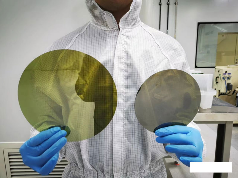
Conductive substrate: By removing various impurities in the crystal, especially shallow level impurities, to achieve the intrinsic high resistivity of the crystal.

Conductive silicon carbide substrate SiC wafer
Conductive silicon carbide power device is through the growth of silicon carbide epitaxial layer on the conductive substrate, the silicon carbide epitaxial sheet is further processed, including the production of Schottky diodes, MOSFET, IGBT, etc., mainly used in electric vehicles, photovoltaic power generation, rail transit, data center, charging and other infrastructure. The performance benefits are as follows:
Enhanced high pressure characteristics. The breakdown electric field strength of silicon carbide is more than 10 times that of silicon, which makes the high pressure resistance of silicon carbide devices significantly higher than that of equivalent silicon devices.
Better high temperature characteristics. Silicon carbide has a higher thermal conductivity than silicon, which makes the device heat dissipation easier and the limit operating temperature higher. High temperature resistance can lead to a significant increase in power density, while reducing the requirements on the cooling system, so that the terminal can be more lightweight and miniaturized.
Lower energy consumption. ① Silicon carbide device has very low on-resistance and low on-loss; (2) The leakage current of silicon carbide devices is significantly reduced than that of silicon devices, thereby reducing power loss; ③ There is no current tailing phenomenon in the turn-off process of silicon carbide devices, and the switching loss is low, which greatly improves the switching frequency of practical applications.
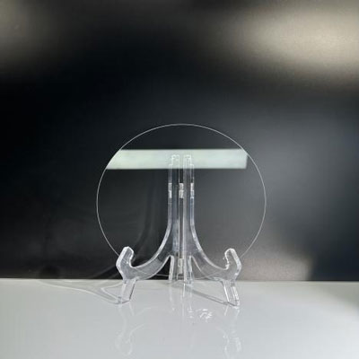
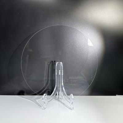
Semi-insulated SiC substrate: N doping is used to accurately control the resistivity of conductive products by calibrating the corresponding relationship between nitrogen doping concentration, growth rate and crystal resistivity.


High purity semi-insulating substrate material
Semi-insulated silicon carbon-based RF devices are further made by growing gallium nitride epitaxial layer on semi-insulated silicon carbide substrate to prepare silicon nitride epitaxial sheet, including HEMT and other gallium nitride RF devices, mainly used in 5G communications, vehicle communications, defense applications, data transmission, aerospace.
The saturated electron drift rate of silicon carbide and gallium nitride materials is 2.0 and 2.5 times that of silicon respectively, so the operating frequency of silicon carbide and gallium nitride devices is greater than that of traditional silicon devices. However, gallium nitride material has the disadvantage of poor heat resistance, while silicon carbide has good heat resistance and thermal conductivity, which can make up for the poor heat resistance of gallium nitride devices, so the industry takes semi-insulated silicon carbide as the substrate, and gan epitaxial layer is grown on the silicon carbide substrate to manufacture RF devices.
If there is infringement, contact delete
Post time: Jul-16-2024
