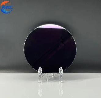
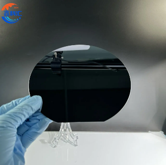
Growing an additional layer of silicon atoms on a silicon wafer substrate has several advantages:
In CMOS silicon processes, epitaxial growth (EPI) on the wafer substrate is a critical process step.
1、Improving crystal quality
Initial substrate defects and impurities: During the manufacturing process, the wafer substrate may have certain defects and impurities. The growth of the epitaxial layer can produce a high-quality monocrystalline silicon layer with low concentrations of defects and impurities on the substrate, which is crucial for subsequent device fabrication.
Uniform crystal structure: Epitaxial growth ensures a more uniform crystal structure, reducing the impact of grain boundaries and defects in the substrate material, thereby improving the overall crystal quality of the wafer.
2、improve electrical performance.
Optimizing device characteristics: By growing an epitaxial layer on the substrate, the doping concentration and type of silicon can be precisely controlled, optimizing the electrical performance of the device. For example, the doping of the epitaxial layer can be finely adjusted to control the threshold voltage of MOSFETs and other electrical parameters.
Reducing leakage current: A high-quality epitaxial layer has a lower defect density, which helps reduce leakage current in devices, thereby improving device performance and reliability.
3、improve electrical performance.
Reducing Feature Size: In smaller process nodes (such as 7nm, 5nm), the feature size of devices continues to shrink, requiring more refined and high-quality materials. Epitaxial growth technology can meet these demands, supporting the manufacturing of high-performance and high-density integrated circuits.
Enhancing Breakdown Voltage: Epitaxial layers can be designed with higher breakdown voltages, which is critical for manufacturing high-power and high-voltage devices. For example, in power devices, epitaxial layers can improve the device's breakdown voltage, increasing the safe operating range.
4、Process Compatibility and Multilayer Structures
Multilayer Structures: Epitaxial growth technology allows for the growth of multilayer structures on substrates, with different layers having varying doping concentrations and types. This is highly beneficial for manufacturing complex CMOS devices and enabling three-dimensional integration.
Compatibility: The epitaxial growth process is highly compatible with existing CMOS manufacturing processes, making it easy to integrate into current manufacturing workflows without the need for significant modifications to the process lines.
Summary: The application of epitaxial growth in CMOS silicon processes primarily aims to enhance wafer crystal quality, optimize device electrical performance, support advanced process nodes, and meet the demands of high-performance and high-density integrated circuit manufacturing. Epitaxial growth technology allows for precise control of material doping and structure, improving the overall performance and reliability of devices.
Post time: Oct-16-2024


