Wafer dicing technology, as a critical step in the semiconductor manufacturing process, is directly linked to chip performance, yield, and production costs.
#01 Background and Significance of Wafer Dicing
1.1 Definition of Wafer Dicing
Wafer dicing (also known as scribing) is an essential step in semiconductor manufacturing, aimed at dividing processed wafers into multiple individual dies. These dies typically contain complete circuit functionality and are the core components ultimately used in the production of electronic devices. As chip designs become more complex and dimensions continue to shrink, the precision and efficiency requirements for wafer dicing technology are becoming increasingly stringent.
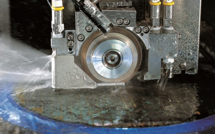
In practical operations, wafer dicing typically utilizes high-precision tools such as diamond blades to ensure that each die remains intact and fully functional. Key steps include preparation before cutting, precise control during the cutting process, and quality inspection after cutting.
Before cutting, the wafer must be marked and positioned to ensure accurate cutting paths. During cutting, parameters such as tool pressure and speed must be strictly controlled to prevent damage to the wafer. After cutting, comprehensive quality inspections are conducted to ensure that every chip meets performance standards.
The fundamental principles of wafer dicing technology encompass not only the selection of cutting equipment and the setting of process parameters but also the influence of the mechanical properties and characteristics of materials on cutting quality. For example, low-k dielectric silicon wafers, due to their inferior mechanical properties, are highly susceptible to stress concentration during cutting, leading to failures such as chipping and cracking. The low hardness and brittleness of low-k materials make them more prone to structural damage under mechanical force or thermal stress, particularly during cutting. The contact between the tool and the wafer surface, coupled with high temperatures, can further exacerbate stress concentration.
With advancements in material science, wafer dicing technology has expanded beyond traditional silicon-based semiconductors to include new materials like gallium nitride (GaN). These new materials, due to their hardness and structural properties, pose new challenges for dicing processes, requiring further improvements in cutting tools and techniques.
As a critical process in the semiconductor industry, wafer dicing continues to be optimized in response to evolving demands and technological advancements, laying the groundwork for future microelectronics and integrated circuit technologies.
Improvements in wafer dicing technology go beyond the development of auxiliary materials and tools. They also encompass process optimization, enhancements in equipment performance, and precise control of dicing parameters. These advancements aim to ensure high precision, efficiency, and stability in the wafer dicing process, meeting the semiconductor industry's need for smaller dimensions, higher integration, and more complex chip structures.
|
mprovement Area |
Specific Measures |
Effects |
| Process Optimization | - Improve initial preparations, such as more accurate wafer positioning and path planning. | - Reduce cutting errors and improve stability. |
| - Minimize cutting errors and enhance stability. | - Adopt real-time monitoring and feedback mechanisms to adjust tool pressure, speed, and temperature. | |
| - Lower wafer breakage rates and improve chip quality. | ||
| Equipment Performance Enhancement | - Utilize high-precision mechanical systems and advanced automation control technology. | - Enhance cutting accuracy and reduce material wastage. |
| - Introduce laser cutting technology suitable for high-hardness material wafers. | - Improve production efficiency and reduce manual errors. | |
| - Increase equipment automation for automatic monitoring and adjustments. | ||
| Precise Parameter Control | - Finely adjust parameters like cutting depth, speed, tool type, and cooling methods. | - Ensure die integrity and electrical performance. |
| - Customize parameters based on wafer material, thickness, and structure. | - Boost yield rates, reduce material waste, and lower production costs. | |
| Strategic Significance | - Continuously explore new technological paths, optimize processes, and enhance equipment capabilities to meet market demands. | - Improve chip manufacturing yield and performance, supporting the development of new materials and advanced chip designs. |
1.2 The Importance of Wafer Dicing
Wafer dicing plays a critical role in the semiconductor manufacturing process, directly impacting subsequent steps as well as the quality and performance of the final product. Its importance can be detailed as follows:
First, the accuracy and consistency of dicing are key to ensuring chip yield and reliability. During manufacturing, wafers undergo multiple processing steps to form numerous intricate circuit structures, which must be precisely divided into individual chips (dies). If there are significant errors in alignment or cutting during the dicing process, the circuits may be damaged, affecting the chip’s functionality and reliability. Therefore, high-precision dicing technology not only ensures the integrity of each chip but also prevents damage to internal circuits, improving the overall yield rate.
Secondly, wafer dicing has a significant impact on production efficiency and cost control. As a crucial step in the manufacturing process, its efficiency directly affects the progress of subsequent steps. By optimizing the dicing process, increasing automation levels, and improving cutting speeds, overall production efficiency can be greatly enhanced.
On the other hand, material wastage during dicing is a critical factor in cost management. Utilizing advanced dicing technologies not only reduces unnecessary material losses during the cutting process but also increases wafer utilization, thereby lowering production costs.
With advancements in semiconductor technology, wafer diameters continue to increase, and circuit densities rise accordingly, placing higher demands on dicing technology. Larger wafers require more precise control of cutting paths, especially in high-density circuit areas, where even minor deviations can render multiple chips defective. Additionally, larger wafers involve more cutting lines and more complex process steps, necessitating further improvements in the precision, consistency, and efficiency of dicing technologies to meet these challenges.
1.3 Wafer Dicing Process
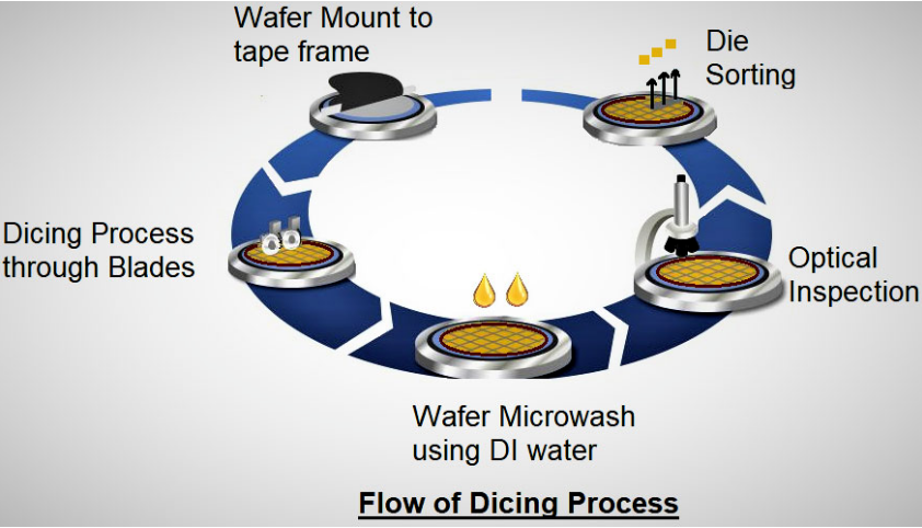
The wafer dicing process encompasses all steps from the preparation phase to the final quality inspection, with each stage being critical to ensuring the quality and performance of the diced chips. Below is a detailed explanation of each phase.
|
Phase |
Detailed Description |
| Preparation Phase | - Wafer Cleaning: Use high-purity water and specialized cleaning agents, combined with ultrasonic or mechanical scrubbing, to remove impurities, particles, and contaminants, ensuring a clean surface. - Precise Positioning: Utilize high-precision equipment to ensure the wafer is accurately divided along the designed cutting paths. - Wafer Fixation: Secure the wafer onto a tape frame to maintain stability during cutting, preventing damage from vibration or movement. |
| Cutting Phase | - Blade Dicing: Employ high-speed rotating diamond-coated blades for physical cutting, suitable for silicon-based materials and cost-effective. - Laser Dicing: Utilize high-energy laser beams for non-contact cutting, ideal for brittle or high-hardness materials like gallium nitride, offering higher precision and less material loss. - New Technologies: Introduce laser and plasma cutting technologies to further improve efficiency and precision while minimizing heat-affected zones. |
| Cleaning Phase | - Use deionized water (DI water) and specialized cleaning agents, combined with ultrasonic or spray cleaning, to remove debris and dust generated during cutting, preventing residues from affecting subsequent processes or chip electrical performance. - High-purity DI water avoids introducing new contaminants, ensuring a clean wafer environment. |
| Inspection Phase | - Optical Inspection: Use optical detection systems combined with AI algorithms to quickly identify defects, ensuring no cracks or chipping in the diced chips, improving inspection efficiency, and reducing human error. - Dimension Measurement: Verify that chip dimensions meet design specifications. - Electrical Performance Testing: Ensure the electrical performance of critical chips meets standards, guaranteeing reliability in subsequent applications. |
| Sorting Phase | - Use robotic arms or vacuum suction cups to separate qualified chips from the tape frame and automatically sort them based on performance, ensuring production efficiency and flexibility while improving precision. |
The wafer cutting process involves wafer cleaning, positioning, cutting, cleaning, inspection, and sorting, with each step being critical. With advancements in automation, laser cutting, and AI inspection technologies, modern wafer cutting systems can achieve higher precision, speed, and lower material loss. In the future, new cutting technologies such as laser and plasma will gradually replace traditional blade cutting to meet the needs of increasingly complex chip designs, further driving the development of semiconductor manufacturing processes.
Wafer Cutting Technology and Its Principles
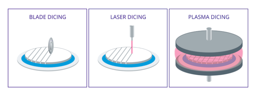
The image illustrates three common wafer cutting technologies: Blade Dicing, Laser Dicing, and Plasma Dicing. Below is a detailed analysis and supplementary explanation of these three techniques:
In semiconductor manufacturing, wafer cutting is a crucial step that requires selecting the appropriate cutting method based on the wafer's thickness. The first step is to determine the wafer's thickness. If the wafer thickness exceeds 100 microns, blade dicing can be chosen as the cutting method. If blade dicing is not suitable, the fracture dicing method can be used, which includes both scribe cutting and blade dicing techniques.
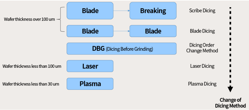
When the wafer thickness is between 30 and 100 microns, the DBG (Dice Before Grinding) method is recommended. In this case, scribe cutting, blade dicing, or adjusting the cutting sequence as needed can be chosen to achieve the best results.
For ultra-thin wafers with a thickness of less than 30 microns, laser cutting becomes the preferred method due to its ability to cut thin wafers precisely without causing excessive damage. If laser cutting cannot meet specific requirements, plasma cutting can be used as an alternative. This flowchart provides a clear decision-making path to ensure the most suitable wafer cutting technology is chosen under different thickness conditions.
2.1 Mechanical Cutting Technology
Mechanical cutting technology is the traditional method in wafer dicing. The core principle is to use a high-speed rotating diamond grinding wheel as a cutting tool to slice the wafer. Key equipment includes an air-bearing spindle, which drives the diamond grinding wheel tool at high speeds to perform precise cutting or grooving along a predefined cutting path. This technology is widely used in the industry due to its low cost, high efficiency, and broad applicability.
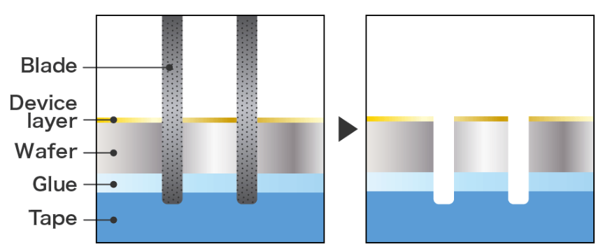
Advantages
The high hardness and wear resistance of diamond grinding wheel tools enable mechanical cutting technology to adapt to the cutting needs of various wafer materials, whether traditional silicon-based materials or newer compound semiconductors. Its operation is simple, with relatively low technical requirements, further promoting its popularity in mass production. Additionally, compared to other cutting methods like laser cutting, mechanical cutting has more controllable costs, making it suitable for high-volume production needs.
Limitations
Despite its numerous advantages, mechanical cutting technology also has limitations. First, due to the physical contact between the tool and the wafer, the cutting precision is relatively limited, often leading to dimensional deviations that can affect the accuracy of subsequent chip packaging and testing. Secondly, defects such as chipping and cracks can easily occur during the mechanical cutting process, which not only affects the yield rate but can also negatively impact the reliability and lifespan of the chips. The mechanical stress-induced damage is particularly detrimental for high-density chip manufacturing, especially when cutting brittle materials, where these issues are more prominent.
Technological Improvements
To overcome these limitations, researchers are continuously optimizing the mechanical cutting process. Key improvements include enhancing the design and material selection of grinding wheels to improve cutting precision and durability. Additionally, optimizing the structural design and control systems of cutting equipment has further improved the stability and automation of the cutting process. These advancements reduce errors caused by human operations and improve the consistency of the cuts. The introduction of advanced inspection and quality control technologies for real-time monitoring of anomalies during the cutting process has also significantly improved cutting reliability and yield.
Future Development and New Technologies
Although mechanical cutting technology still holds a significant position in wafer cutting, new cutting technologies are rapidly advancing as semiconductor processes evolve. For example, the application of thermal laser cutting technology provides new solutions to the precision and defect issues in mechanical cutting. This non-contact cutting method reduces the physical stress on the wafer, significantly lowering the incidence of chipping and cracking, especially when cutting more brittle materials. In the future, the integration of mechanical cutting technology with emerging cutting techniques will provide semiconductor manufacturing with more options and flexibility, further enhancing manufacturing efficiency and chip quality.
In conclusion, although mechanical cutting technology has certain drawbacks, continuous technological improvements and its integration with new cutting techniques allow it to still play an important role in semiconductor manufacturing and maintain its competitiveness in future processes.
2.2 Laser Cutting Technology
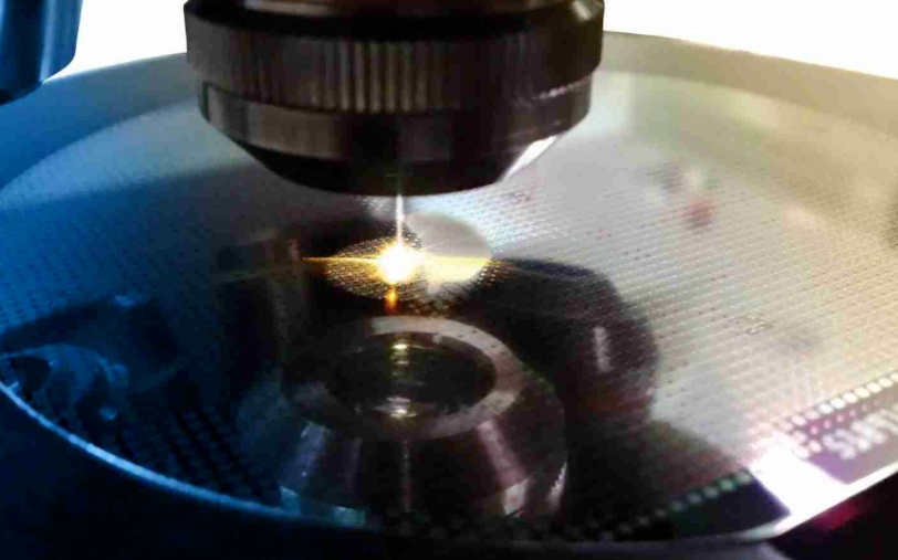
Laser cutting technology, as a new method in wafer cutting, has gradually gained widespread attention in the semiconductor industry due to its high precision, lack of mechanical contact damage, and rapid cutting capabilities. This technology uses the high energy density and focusing ability of a laser beam to create a small heat-affected zone on the wafer material's surface. When the laser beam is applied to the wafer, the thermal stress generated causes the material to fracture at the designated location, achieving precise cutting.
Advantages of Laser Cutting Technology
• High Precision: The laser beam's precise positioning capability allows for micron or even nanometer-level cutting precision, meeting the requirements of modern high-precision, high-density integrated circuit manufacturing.
• No Mechanical Contact: Laser cutting avoids physical contact with the wafer, preventing common issues in mechanical cutting, such as chipping and cracking, significantly improving the yield rate and reliability of the chips.
• Fast Cutting Speed: The high speed of laser cutting contributes to increased production efficiency, making it especially suitable for large-scale, high-speed production scenarios.
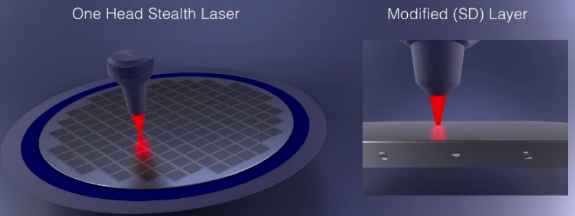
Challenges Faced
• High Equipment Cost: The initial investment for laser cutting equipment is high, which presents economic pressure, especially for small to medium-sized production enterprises.
• Complex Process Control: Laser cutting requires precise control of several parameters, including energy density, focus position, and cutting speed, making the process complex.
• Heat-Affected Zone Issues: Although laser cutting's non-contact nature reduces mechanical damage, the thermal stress caused by the heat-affected zone (HAZ) can negatively impact the wafer material's properties. Further optimization of the process is needed to minimize this effect.
Technological Improvement Directions
To address these challenges, researchers are focusing on lowering equipment costs, improving cutting efficiency, and optimizing the process flow.
• Efficient Lasers and Optical Systems: By developing more efficient lasers and advanced optical systems, it is possible to lower equipment costs while enhancing cutting precision and speed.
• Optimizing Process Parameters: In-depth research on the interaction between lasers and wafer materials is being conducted to improve processes that reduce the heat-affected zone, thereby improving cutting quality.
• Intelligent Control Systems: The development of intelligent control technologies aims to automate and optimize the laser cutting process, improving its stability and consistency.
Laser cutting technology is particularly effective in ultra-thin wafers and high-precision cutting scenarios. As wafer sizes increase and circuit densities rise, traditional mechanical cutting methods struggle to meet the high-precision and high-efficiency demands of modern semiconductor manufacturing. Due to its unique advantages, laser cutting is becoming the preferred solution in these fields.
Although laser cutting technology still faces challenges such as high equipment costs and process complexity, its unique advantages in high precision and non-contact damage make it an important direction for development in semiconductor manufacturing. As laser technology and intelligent control systems continue to advance, laser cutting is expected to further improve wafer cutting efficiency and quality, driving the continuous development of the semiconductor industry.
2.3 Plasma Cutting Technology
Plasma cutting technology, as an emerging wafer dicing method, has gained significant attention in recent years. This technology uses high-energy plasma beams to precisely cut wafers by controlling the energy, speed, and cutting path of the plasma beam, achieving optimal cutting results.
Working Principle and Advantages
The process of plasma cutting relies on a high-temperature, high-energy plasma beam generated by the equipment. This beam can heat the wafer material to its melting or vaporization point in a very short amount of time, enabling fast cutting. Compared to traditional mechanical or laser cutting, plasma cutting is faster and produces a smaller heat-affected zone, effectively reducing the occurrence of cracks and damage during cutting.
In practical applications, plasma cutting technology is particularly adept at handling wafers with complex shapes. Its high-energy, adjustable plasma beam can easily cut irregularly shaped wafers with high precision. Therefore, in microelectronics manufacturing, especially in customized and small-batch production of high-end chips, this technology shows great promise for widespread use.
Challenges and Limitations
Despite the many advantages of plasma cutting technology, it also faces some challenges.
• Complex Process: The plasma cutting process is complex and requires high-precision equipment and experienced operators to ensure accuracy and stability in cutting.
• Environmental Control and Safety: The high-temperature, high-energy nature of the plasma beam requires stringent environmental control and safety measures, which increases the complexity and cost of implementation.
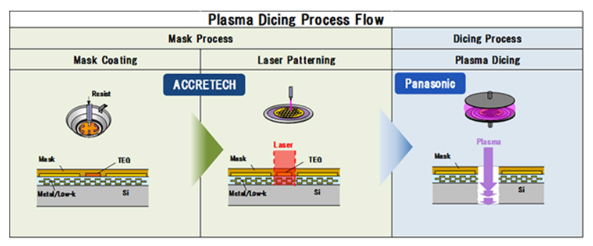
Future Development Directions
With technological advancements, the challenges associated with plasma cutting are expected to be gradually overcome. By developing smarter and more stable cutting equipment, dependence on manual operations can be reduced, thereby improving production efficiency. At the same time, optimizing process parameters and the cutting environment will help lower safety risks and operational costs.
In the semiconductor industry, innovations in wafer cutting and dicing technology are crucial to driving the industry's development. Plasma cutting technology, with its high precision, efficiency, and ability to handle complex wafer shapes, has emerged as a significant new player in this field. Although some challenges remain, these issues will be gradually addressed with continued technological innovation, bringing more possibilities and opportunities to semiconductor manufacturing.
The application prospects of plasma cutting technology are vast, and it is expected to play a more important role in semiconductor manufacturing in the future. Through continuous technological innovation and optimization, plasma cutting will not only address existing challenges but also become a powerful driver of the semiconductor industry's growth.
2.4 Cutting Quality and Influencing Factors
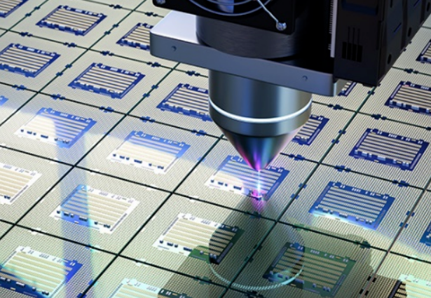
Wafer cutting quality is critical for the subsequent chip packaging, testing, and the overall performance and reliability of the final product. Common issues encountered during cutting include cracks, chipping, and cutting deviations. These problems are influenced by several factors working together.
|
Category |
Content |
Impact |
| Process Parameters | Cutting speed, feed rate, and cutting depth directly affect the stability and precision of the cutting process. Improper settings can lead to stress concentration and excessive heat-affected zone, resulting in cracks and chipping. Adjusting parameters appropriately based on wafer material, thickness, and cutting requirements is key to achieving the desired cutting results. | The right process parameters ensure precise cutting and reduce the risk of defects like cracks and chipping. |
| Equipment and Material Factors | - Blade Quality: The material, hardness, and wear resistance of the blade influence the smoothness of the cutting process and the flatness of the cut surface. Poor-quality blades increase friction and thermal stress, potentially leading to cracks or chipping. Choosing the right blade material is crucial. - Coolant Performance: Coolants help reduce cutting temperature, minimize friction, and clear debris. Ineffective coolant can lead to high temperatures and debris buildup, impacting cutting quality and efficiency. Selecting efficient and environmentally friendly coolants is vital. |
Blade quality affects the precision and smoothness of the cut. Ineffective coolant can result in poor cutting quality and efficiency, highlighting the need for optimal coolant use. |
| Process Control and Quality Inspection | - Process Control: Real-time monitoring and adjustment of key cutting parameters to ensure stability and consistency in the cutting process. - Quality Inspection: Post-cutting appearance checks, dimensional measurements, and electrical performance testing help identify and address quality issues promptly, improving cutting accuracy and consistency. |
Proper process control and quality inspection help ensure consistent, high-quality cutting results and early detection of potential issues. |
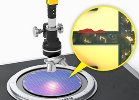
Improving Cutting Quality
Improving cutting quality requires a comprehensive approach that takes into account process parameters, equipment and material selection, process control, and inspection. By continually refining cutting technologies and optimizing process methods, the precision and stability of wafer cutting can be further enhanced, providing more reliable technical support for the semiconductor manufacturing industry.
#03 Post-Cutting Handling and Testing
3.1 Cleaning and Drying
The cleaning and drying steps after wafer cutting are critical for ensuring chip quality and the smooth progression of subsequent processes. During this stage, it is essential to thoroughly remove silicon debris, coolant residue, and other contaminants generated during cutting. It is equally important to ensure that the chips are not damaged during the cleaning process, and after drying, ensure that no moisture remains on the chip surface to prevent issues such as corrosion or electrostatic discharge.
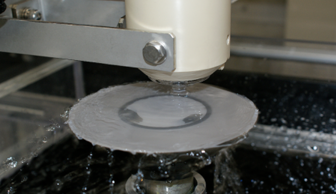
Post-Cutting Handling: Cleaning and Drying Process
|
Process Step |
Content |
Impact |
| Cleaning Process | - Method: Use specialized cleaning agents and pure water, combined with ultrasonic or mechanical brushing techniques for cleaning. | Ensures thorough removal of contaminants and prevents damage to the chips during cleaning. |
| - Cleaning Agent Selection: Choose based on wafer material and contaminant type to ensure effective cleaning without damaging the chip. | Proper agent selection is key for effective cleaning and chip protection. | |
| - Parameter Control: Strictly control cleaning temperature, time, and cleaning solution concentration to prevent quality issues caused by improper cleaning. | Controls help to avoid damaging the wafer or leaving contaminants behind, ensuring consistent quality. | |
| Drying Process | - Traditional Methods: Natural air drying and hot air drying, which have low efficiency and can lead to static electricity buildup. | May result in slower drying times and potential static issues. |
| - Modern Technologies: Use advanced technologies such as vacuum drying and infrared drying to ensure that chips dry quickly and avoid harmful effects. | Faster and more efficient drying process, reducing risk of static discharge or moisture-related issues. | |
| Equipment Selection & Maintenance | - Equipment Selection: High-performance cleaning and drying machines improve processing efficiency and finely control potential issues during handling. | High-quality machines ensure better processing and reduce the likelihood of errors during cleaning and drying. |
| - Equipment Maintenance: Regular inspection and maintenance of equipment ensure it remains in optimal working condition, guaranteeing chip quality. | Proper maintenance prevents equipment failures, ensuring reliable and high-quality processing. |
Post-Cutting Cleaning and Drying
The cleaning and drying steps after wafer cutting are complex and delicate processes that require careful consideration of multiple factors to ensure the final processing outcome. By using scientific methods and rigorous procedures, it is possible to ensure that each chip enters the subsequent packaging and testing stages in optimal condition.
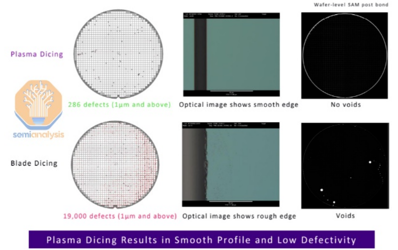
Post-Cutting Inspection and Testing
|
Step |
Content |
Impact |
| Inspection Step | 1. Visual Inspection: Use visual or automated inspection equipment to check for visible defects like cracks, chipping, or contamination on the chip surface. Quickly identify physically damaged chips to avoid waste. | Helps in identifying and eliminating defective chips early in the process, reducing material loss. |
| 2. Size Measurement: Use precision measuring devices to accurately measure chip dimensions, ensuring the cut size meets design specifications and preventing performance issues or packaging difficulties. | Ensures chips are within required size limits, preventing performance degradation or assembly problems. | |
| 3. Electrical Performance Testing: Evaluate key electrical parameters such as resistance, capacitance, and inductance, to identify non-compliant chips and ensure only performance-qualified chips proceed to the next stage. | Ensures only functional and performance-tested chips move forward in the process, reducing the risk of failure in later stages. | |
| Testing Step | 1. Functional Testing: Verify that the basic functionality of the chip works as intended, identifying and eliminating chips with functional abnormalities. | Ensures chips meet basic operational requirements before progressing to later stages. |
| 2. Reliability Testing: Evaluate chip performance stability under prolonged use or harsh environments, typically involving high-temperature aging, low-temperature testing, and humidity testing to simulate real-world extreme conditions. | Ensures chips can reliably function under a range of environmental conditions, improving product longevity and stability. | |
| 3. Compatibility Testing: Verify that the chip works properly with other components or systems, ensuring there are no faults or performance degradation due to incompatibility. | Ensures smooth operation in real-world applications by preventing compatibility issues. |
3.3 Packaging and Storage
After wafer cutting, the chips are a crucial output of the semiconductor manufacturing process, and their packaging and storage stages are equally important. Proper packaging and storage measures are essential not only for ensuring the safety and stability of the chips during transportation and storage but also for providing strong support for subsequent production, testing, and packaging stages.
Summary of Inspection and Testing Stages:
The inspection and testing steps for chips after wafer cutting cover a range of aspects, including visual inspection, size measurement, electrical performance testing, functional testing, reliability testing, and compatibility testing. These steps are interconnected and complementary, forming a solid barrier to ensure product quality and reliability. Through strict inspection and testing procedures, potential issues can be identified and resolved promptly, ensuring the final product meets customer requirements and expectations.
|
Aspect |
Content |
| Packaging Measures | 1. Anti-static: Packaging materials should have excellent anti-static properties to prevent static electricity from damaging the devices or affecting their performance. |
| 2. Moisture-proof: Packaging materials should have good moisture resistance to prevent corrosion and deterioration of electrical performance caused by humidity. | |
| 3. Shockproof: Packaging materials should provide effective shock absorption to protect the chips from vibration and impact during transportation. | |
| Storage Environment | 1. Humidity Control: Strictly control humidity within an appropriate range to prevent moisture absorption and corrosion caused by excessive humidity or static issues caused by low humidity. |
| 2. Cleanliness: Maintain a clean storage environment to avoid contamination of chips by dust and impurities. | |
| 3. Temperature Control: Set a reasonable temperature range and maintain temperature stability to prevent accelerated aging due to excessive heat or condensation problems caused by low temperatures. | |
| Regular Inspection | Regularly inspect and evaluate stored chips, using visual inspections, size measurements, and electrical performance tests to identify and address potential issues in a timely manner. Based on storage time and conditions, plan the use of chips to ensure they are used in optimal condition. |
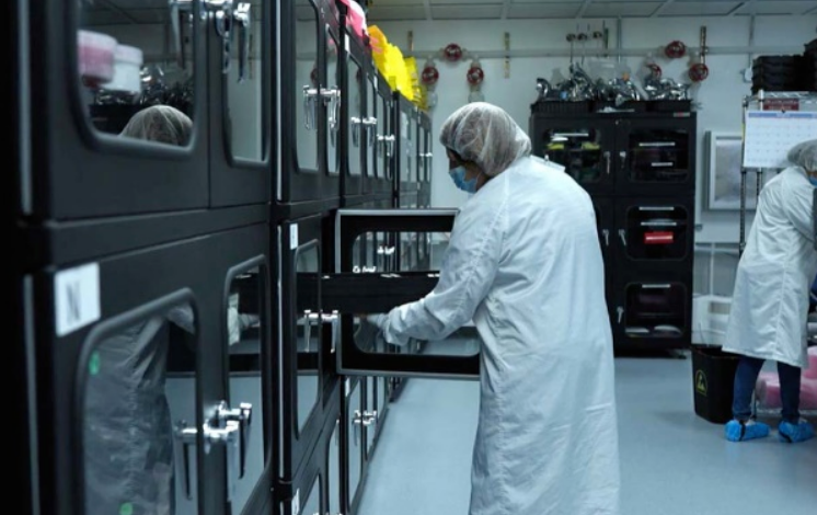
The issue of microcracks and damage during the wafer dicing process is a significant challenge in semiconductor manufacturing. The cutting stress is the primary cause of this phenomenon, as it creates tiny cracks and damage on the wafer surface, leading to increased manufacturing costs and a decrease in product quality.
In order to address this challenge, it is crucial to minimize cutting stress and implement optimized cutting techniques, tools, and conditions. Careful attention to factors such as blade material, cutting speed, pressure, and cooling methods can help reduce the formation of microcracks and improve the overall yield of the process. Additionally, ongoing research into more advanced cutting technologies, such as laser dicing, is exploring ways to further mitigate these issues.
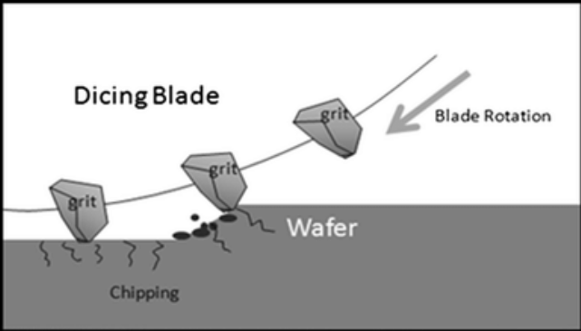
As a fragile material, wafers are prone to internal structural changes when subjected to mechanical, thermal, or chemical stress, leading to the formation of microcracks. Although these cracks may not be immediately noticeable, they can expand and cause more severe damage as the manufacturing process progresses. This issue becomes especially problematic during subsequent packaging and testing stages, where temperature fluctuations and additional mechanical stresses can cause these microcracks to evolve into visible fractures, potentially leading to chip failure.
To mitigate this risk, it is essential to control the cutting process carefully by optimizing parameters such as cutting speed, pressure, and temperature. Using less aggressive cutting methods, such as laser dicing, can reduce the mechanical stress on the wafer and minimize the formation of microcracks. Additionally, implementing advanced inspection methods like infrared scanning or X-ray imaging during the wafer dicing process can help detect these early-stage cracks before they cause further damage.
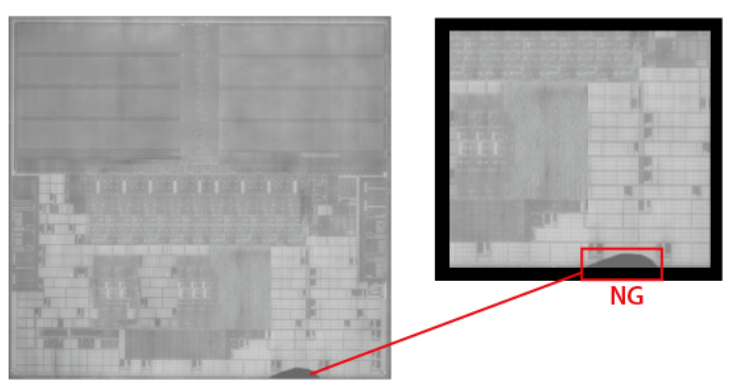
The damage to the wafer surface is a significant concern in the dicing process, as it can have a direct impact on the chip's performance and reliability. Such damage can be caused by improper use of cutting tools, incorrect cutting parameters, or material defects inherent in the wafer itself. Regardless of the cause, these damages can lead to alterations in the electrical resistance or capacitance of the circuit, affecting overall performance.
To address these issues, two key strategies are being explored:
1.Optimizing cutting tools and parameters: By using sharper blades, adjusting cutting speed, and modifying cutting depth, stress concentration during the cutting process can be minimized, thus reducing the potential for damage.
2.Exploring new cutting technologies: Advanced techniques like laser cutting and plasma cutting offer improved precision while potentially reducing the level of damage inflicted on the wafer. These technologies are being studied to find ways to achieve high cutting accuracy while minimizing thermal and mechanical stress on the wafer.
Thermal Impact Area and Its Effects on Performance
In thermal cutting processes such as laser and plasma cutting, high temperatures inevitably create a thermal impact zone on the wafer's surface. This area, where the temperature gradient is significant, can alter the material's properties, affecting the final performance of the chip.
Impact of the Thermal Affected Zone (TAZ):
Crystal Structure Changes: Under high temperatures, atoms within the wafer material may rearrange, causing distortions in the crystal structure. This distortion weakens the material, reducing its mechanical strength and stability, which increases the risk of chip failure during usage.
Changes in Electrical Properties: High temperatures can alter the carrier concentration and mobility in semiconductor materials, affecting the chip’s electrical conductivity and current transmission efficiency. These changes may lead to a decline in chip performance, potentially making it unsuitable for its intended purpose.
To mitigate these effects, controlling the temperature during cutting, optimizing the cutting parameters, and exploring methods like cooling jets or post-processing treatments are essential strategies to reduce the extent of the thermal impact and maintain material integrity.
Overall, both microcracks and thermal impact zones are crucial challenges in wafer dicing technology. Continued research, alongside technological advancements and quality control measures, will be necessary to improve the quality of semiconductor products and enhance their market competitiveness.
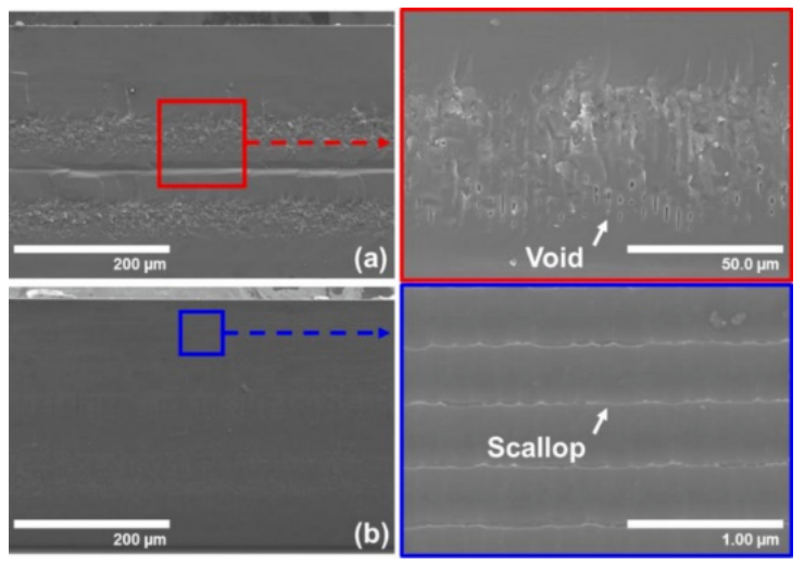
Measures to Control the Thermal Impact Zone:
Optimizing Cutting Process Parameters: Reducing the cutting speed and power can effectively minimize the size of the thermal impact zone (TAZ). This helps in controlling the amount of heat generated during the cutting process, which directly impacts the material properties of the wafer.
Advanced Cooling Technologies: The application of technologies like liquid nitrogen cooling and microfluidic cooling can significantly limit the range of the thermal impact zone. These cooling methods help dissipate heat more efficiently, thus preserving the wafer's material properties and minimizing thermal damage.
Material Selection: Researchers are exploring new materials, such as carbon nanotubes and graphene, which possess excellent thermal conductivity and mechanical strength. These materials can reduce the thermal impact zone while improving the overall performance of the chips.
In summary, although the thermal impact zone is an inevitable consequence of thermal cutting technologies, it can be effectively controlled through optimized processing techniques and material selection. Future research will likely focus on fine-tuning and automating thermal cutting processes to achieve more efficient and precise wafer dicing.
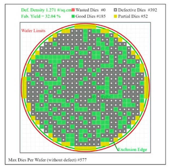
Balance Strategy:
Achieving the optimal balance between wafer yield and production efficiency is a continual challenge in wafer dicing technology. Manufacturers need to consider multiple factors, such as market demand, production costs, and product quality, to develop a rational production strategy and process parameters. At the same time, introducing advanced cutting equipment, improving operator skills, and enhancing raw material quality control are essential to maintaining or even improving yield while increasing production efficiency.
Future Challenges and Opportunities:
With the advancement of semiconductor technology, wafer cutting faces new challenges and opportunities. As chip sizes shrink and integration increases, the demands on cutting precision and quality grow significantly. Simultaneously, emerging technologies provide new ideas for the development of wafer cutting techniques. Manufacturers must stay attuned to market dynamics and technological trends, continuously adjusting and optimizing production strategies and process parameters to meet market changes and technological demands.
In conclusion, by integrating considerations of market demand, production costs, and product quality, and by introducing advanced equipment and technology, enhancing operator skills, and strengthening raw material control, manufacturers can achieve the best balance between wafer yield and production efficiency during wafer dicing, leading to efficient and high-quality semiconductor product production.
Future Outlook:
With rapid technological advancements, semiconductor technology is progressing at an unprecedented pace. As a critical step in semiconductor manufacturing, wafer cutting technology is poised for exciting new developments. Looking ahead, wafer cutting technology is expected to achieve significant improvements in precision, efficiency, and cost, injecting new vitality into the continued growth of the semiconductor industry.
Increasing Precision:
In the pursuit of higher precision, wafer cutting technology will continually push the limits of existing processes. By deeply studying the physical and chemical mechanisms of the cutting process and precisely controlling cutting parameters, finer cutting results will be achieved to meet increasingly complex circuit design requirements. Additionally, the exploration of new materials and cutting methods will significantly improve yield and quality.
Enhancing Efficiency:
New wafer cutting equipment will focus on smart and automated design. The introduction of advanced control systems and algorithms will enable equipment to automatically adjust cutting parameters to accommodate different materials and design requirements, thus significantly improving production efficiency. Innovations such as multi-wafer cutting technology and rapid blade replacement systems will play a crucial role in enhancing efficiency.
Reducing Costs:
Reducing costs is a key direction for the development of wafer cutting technology. As new materials and cutting methods are developed, equipment costs and maintenance expenses are expected to be effectively controlled. Additionally, optimizing production processes and reducing scrap rates will further reduce waste during manufacturing, leading to a decrease in overall production costs.
Smart Manufacturing and IoT:
The integration of smart manufacturing and the Internet of Things (IoT) technologies will bring transformative changes to wafer cutting technology. Through interconnectivity and data sharing between devices, every step of the production process can be monitored and optimized in real time. This not only improves production efficiency and product quality but also provides companies with more accurate market forecasting and decision-making support.
In the future, wafer cutting technology will make remarkable advances in precision, efficiency, and cost. These advancements will drive the continued development of the semiconductor industry and bring more technological innovations and conveniences to human society.
Post time: Nov-19-2024
