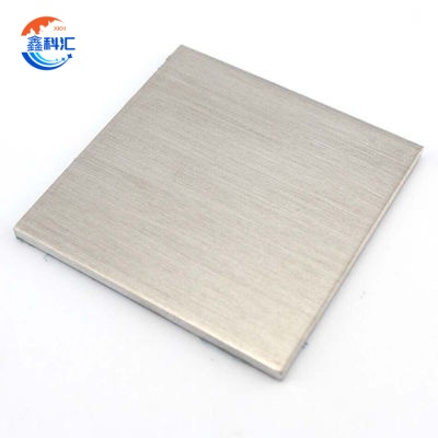
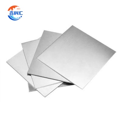
Ni Substrate/wafer single crystal cubic structure a=3.25A density 8.91
Specification
The crystallographic orientations of Ni substrates, such as <100>, <110>, and <111>, play a crucial role in determining the material’s surface and interaction properties. These orientations provide lattice matching capabilities with different thin-film materials, supporting precise growth of epitaxial layers. In addition, nickel's corrosion resistance makes it durable in harsh environments, which is beneficial for applications in aerospace, marine, and chemical processing. Its mechanical strength further ensures that Ni substrates can withstand the rigors of physical processing and experimentation without degrading, providing a stable base for thin-film deposition and coating technologies. This combination of thermal, electrical, and mechanical properties makes Ni substrates essential for advanced research in nanotechnology, surface science, and electronics.
Characteristics of nickel can include high hardness and strength, which can be as hard as 48-55 HRC. Good corrosion resistance, especially to acid and alkali and other chemical media have excellent corrosion resistance. Good electrical conductivity and magnetism, is one of the main components of the manufacture of electromagnetic alloys.
Nickel can be used in many fields, such as as a conductive material for electronic components and as a contact material. Used to manufacture batteries, motors, transformers and other electromagnetic equipment. Used in electronic connectors, transmission lines and other electrical systems. As a structural material for chemical equipment, containers, pipelines, etc. Used to manufacture chemical reaction equipment with high corrosion resistance requirements. It is used in pharmaceutical, petrochemical and other fields where corrosion resistance of materials is strictly required.
Nickel (Ni) substrates, due to their versatile physical, chemical, and crystallographic properties, find numerous applications across a variety of scientific and industrial fields. Below are some of the key applications of Ni substrates: Nickel substrates are extensively used in the deposition of thin films and epitaxial layers. The specific crystallographic orientations of Ni substrates, such as <100>, <110>, and <111>, provide lattice matching with various materials, allowing for precise and controlled growth of thin films. Ni substrates are often used in the development of magnetic storage devices, sensors, and spintronic devices, where controlling electron spin is key to improving device performance. Nickel is an excellent catalyst for hydrogen evolution reactions (HER) and oxygen evolution reactions (OER), which are critical in water splitting and fuel cell technology. Ni substrates are often used as support materials for catalytic coatings in these applications, contributing to efficient energy conversion processes.
We can customize various specifications, thicknesses and shapes of Ni Single crystal substrate according to customers' specific requirements.
Detailed Diagram


