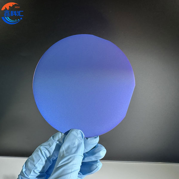
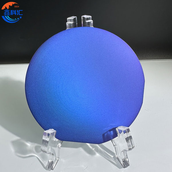
P-type SiC substrate SiC wafer Dia2inch new product


P-type silicon carbide substrates are commonly used to make power devices, such as Insulate-Gate Bipolar transistors (IGBTs).
IGBT= MOSFET+BJT, which is an on-off switch. MOSFET=IGFET(metal oxide semiconductor field effect tube, or insulated gate type field effect transistor). BJT(Bipolar Junction Transistor, also known as the transistor), bipolar means that there are two kinds of electron and hole carriers involved in the conduction process at work, generally there is PN junction involved in conduction.
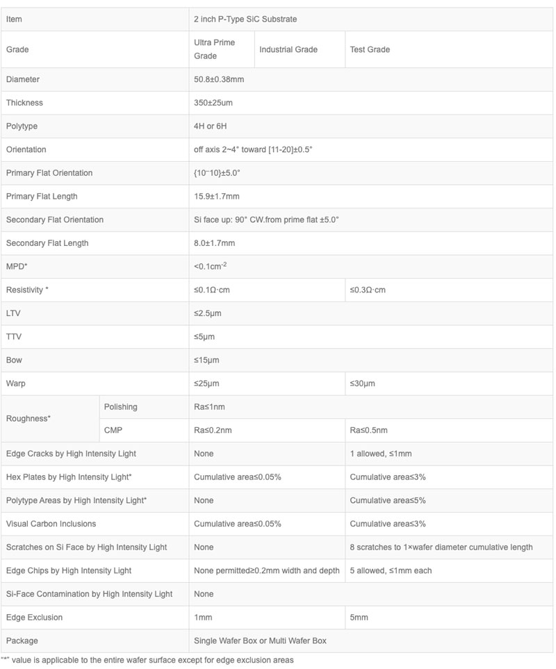
The 2-inch p-type silicon carbide (SiC) wafer is in 4H or 6H polytype. It has similar properties to n-type silicon carbide (SiC) wafers, such as high temperature resistance, high thermal conductivity, and high electrical conductivity. p-type SiC substrates are commonly used in the fabrication of power devices, particularly for the fabrication of insulated-gate bipolar transistors (IGBTs). the design of IGBTs typically involves P-N junctions, where p-type SiC is advantageous for controlling the behavior of the device.
Detailed Diagram
Products categories
-

SiC crystal growth furnace SiC Ingot growing 4i...
-

3inch 76.2mm 4H-Semi SiC substrate wafer Silico...
-
2 inch 50.8mm Sapphire Wafer C-Plane M-plane R-...
-
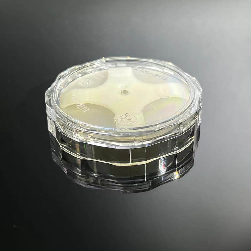
2inch 50.8mm single wafer carrier box of PC and PP
-

2inch Silicon Carbide Wafer 6H-N Type Prime Gra...
-

GaN-on-Diamond Wafers 4inch 6inch Total epi thi...