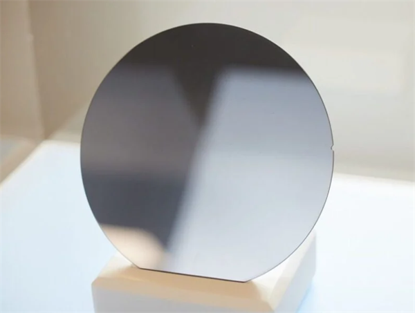
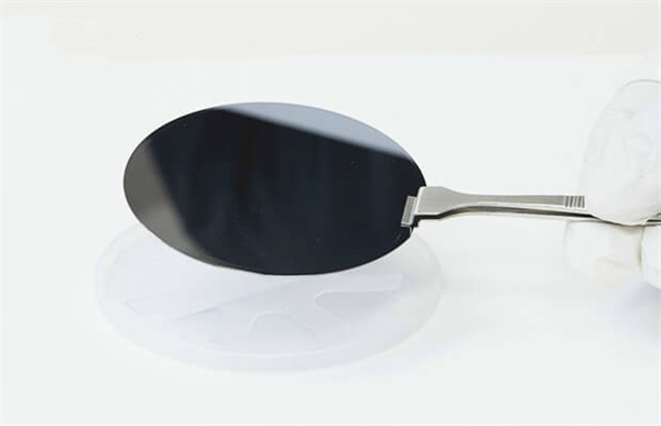
P-type SiC wafer 4H/6H-P 3C-N 6inch thickeness 350 μm with Primary Flat Orientation


Specification4H/6H-P Type SiC Composite Substrates Common parameter table
6 inch diameter Silicon Carbide (SiC) Substrate Specification
| Grade | Zero MPD ProductionGrade (Z Grade) | Standard ProductionGrade (P Grade) | Dummy Grade (D Grade) | ||
| Diameter | 145.5 mm~150.0 mm | ||||
| Thickness | 350 μm ± 25 μm | ||||
| Wafer Orientation | -Off axis: 2.0°-4.0°toward [1120] ± 0.5° for 4H/6H-P, On axis:〈111〉± 0.5° for 3C-N | ||||
| Micropipe Density | 0 cm-2 | ||||
| Resistivity | p-type 4H/6H-P | ≤0.1 Ωꞏcm | ≤0.3 Ωꞏcm | ||
| n-type 3C-N | ≤0.8 mΩꞏcm | ≤1 m Ωꞏcm | |||
| Primary Flat Orientation | 4H/6H-P | -{1010} ± 5.0° | |||
| 3C-N | -{110} ± 5.0° | ||||
| Primary Flat Length | 32.5 mm ± 2.0 mm | ||||
| Secondary Flat Length | 18.0 mm ± 2.0 mm | ||||
| Secondary Flat Orientation | Silicon face up: 90° CW. from Prime flat ± 5.0° | ||||
| Edge Exclusion | 3 mm | 6 mm | |||
| LTV/TTV/Bow /Warp | ≤2.5 μm/≤5 μm/≤15 μm/≤30 μm | ≤10 μm/≤15 μm/≤25 μm/≤40 μm | |||
| Roughness | Polish Ra≤1 nm | ||||
| CMP Ra≤0.2 nm | Ra≤0.5 nm | ||||
| Edge Cracks By High Intensity Light | None | Cumulative length ≤ 10 mm, single length≤2 mm | |||
| Hex Plates By High Intensity Light | Cumulative area ≤0.05% | Cumulative area ≤0.1% | |||
| Polytype Areas By High Intensity Light | None | Cumulative area≤3% | |||
| Visual Carbon Inclusions | Cumulative area ≤0.05% | Cumulative area ≤3% | |||
| Silicon Surface Scratches By High Intensity Light | None | Cumulative length≤1×wafer diameter | |||
| Edge Chips High By Intensity Light | None permitted ≥0.2mm width and depth | 5 allowed, ≤1 mm each | |||
| Silicon Surface Contamination By High Intensity | None | ||||
| Packaging | Multi-wafer Cassette or Single Wafer Container | ||||
Notes:
※ Defects limits apply to entire wafer surface except for the edge exclusion area. # The scratches should be checked on Si face o
The P-type SiC wafer, 4H/6H-P 3C-N, with its 6-inch size and 350 μm thickness, plays a crucial role in the industrial production of high-performance power electronics. Its excellent thermal conductivity and high breakdown voltage make it ideal for manufacturing components such as power switches, diodes, and transistors used in high-temperature environments like electric vehicles, power grids, and renewable energy systems. The wafer’s ability to operate efficiently in harsh conditions ensures reliable performance in industrial applications requiring high power density and energy efficiency. Additionally, its primary flat orientation aids in precise alignment during device fabrication, enhancing production efficiency and product consistency.
The advantages of N-type SiC composite substrates include
- High Thermal Conductivity: P-type SiC wafers efficiently dissipate heat, making them ideal for high-temperature applications.
- High Breakdown Voltage: Capable of withstanding high voltages, ensuring reliability in power electronics and high-voltage devices.
- Resistance to Harsh Environments: Excellent durability in extreme conditions, such as high temperatures and corrosive environments.
- Efficient Power Conversion: The P-type doping facilitates efficient power handling, making the wafer suitable for energy conversion systems.
- Primary Flat Orientation: Ensures precise alignment during manufacturing, improving device accuracy and consistency.
- Thin Structure (350 μm): The wafer's optimal thickness supports integration into advanced, space-constrained electronic devices.
Overall, the P-type SiC wafer, 4H/6H-P 3C-N, offers a range of advantages that make it highly suitable for industrial and electronic applications. Its high thermal conductivity and breakdown voltage enable reliable operation in high-temperature and high-voltage environments, while its resistance to harsh conditions ensures durability. The P-type doping allows for efficient power conversion, making it ideal for power electronics and energy systems. Additionally, the wafer's primary flat orientation ensures precise alignment during the manufacturing process, enhancing production consistency. With a thickness of 350 μm, it is well-suited for integration into advanced, compact devices.
Detailed Diagram