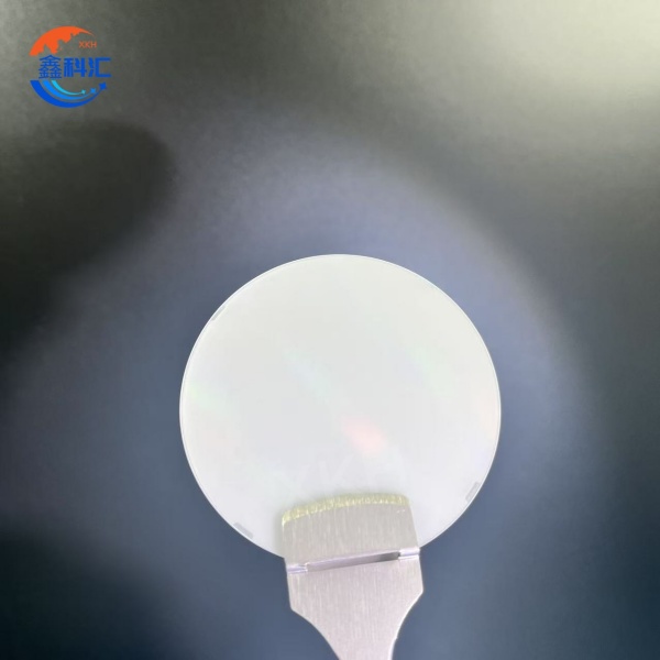
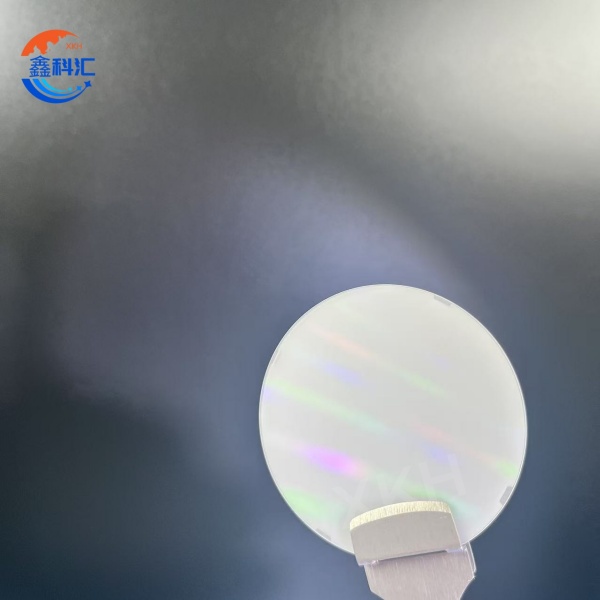
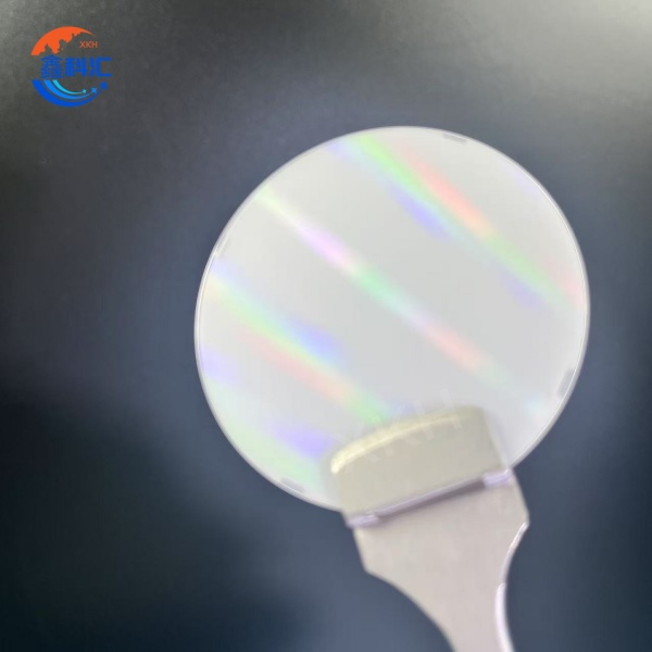
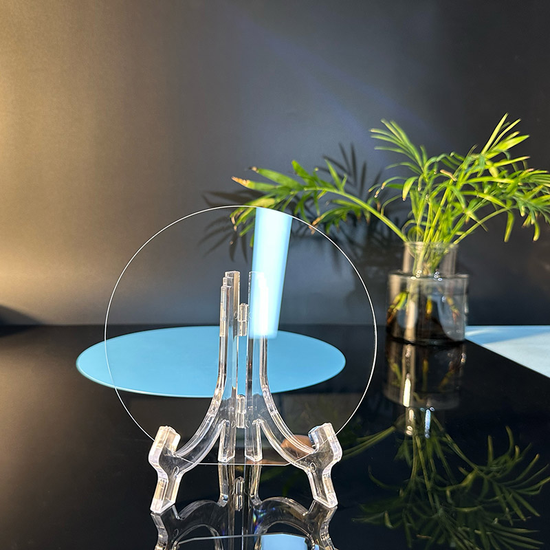
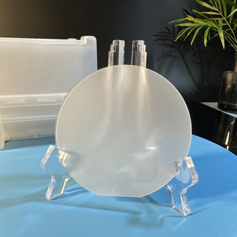
Patterned Sapphire Substrate PSS 2inch 4inch 6inch ICP dry etching can be used for LED chips


Core characteristic
1. Material characteristics: The substrate material is a single crystal sapphire (Al₂O₃), with high hardness, high heat resistance and chemical stability.
2. Surface structure: The surface is formed by photolithography and etching into periodic micro-nano structures, such as cones, pyramids or hexagonal arrays.
3. Optical performance: Through the surface patterning design, the total reflection of light at the interface is reduced, and the light extraction efficiency is improved.
4. Thermal performance: Sapphire substrate has excellent thermal conductivity, suitable for high power LED applications.
5. Size specifications: Common sizes are 2 inches (50.8mm), 4 inches (100mm) and 6 inches (150mm).
Main application areas
1. LED manufacturing:
Improved light extraction efficiency: PSS reduces light loss through patterning design, significantly improving LED brightness and luminous efficiency.
Improved epitaxial growth quality: The patterned structure provides a better growth base for GaN epitaxial layers and improves LED performance.
2. Laser Diode (LD) :
High power lasers: The high thermal conductivity and stability of PSS are suitable for high power laser diodes, improving heat dissipation performance and reliability.
Low threshold current: Optimize epitaxial growth, reduce the threshold current of the laser diode, and improve efficiency.
3. Photodetector:
High sensitivity: The high light transmission and low defect density of the PSS improve the sensitivity and response speed of the photodetector.
Wide spectral response: suitable for photoelectric detection in the ultraviolet to visible range.
4. Power electronics:
High voltage resistance: Sapphire's high insulation and thermal stability are suitable for high voltage power devices.
Efficient heat dissipation: High thermal conductivity improves heat dissipation performance of power devices and prolongs service life.
5. Rf devices:
High frequency performance: The low dielectric loss and high thermal stability of PSS are suitable for high frequency RF devices.
Low noise: High flatness and low defect density reduce device noise and improve signal quality.
6. Biosensors:
High sensitivity detection: The high light transmission and chemical stability of PSS are suitable for high sensitivity biosensors.
Biocompatibility: The biocompatibility of sapphire makes it suitable for medical and biodetection applications.
Patterned sapphire substrate (PSS) with GaN epitaxial material:
Patterned sapphire substrate (PSS) is an ideal substrate for GaN (gallium nitride) epitaxial growth. The lattice constant of sapphire is close to GaN, which can reduce lattice mismatches and defects in epitaxial growth. The micro-nano structure of the PSS surface not only improves the light extraction efficiency, but also improves the crystal quality of the GaN epitaxial layer, thereby improving the performance and reliability of the LED.
Technical parameters
| Item | Patterned Sapphire Substrate(2~6inch) | ||
| Diameter | 50.8 ± 0.1 mm | 100.0 ± 0.2 mm | 150.0 ± 0.3 mm |
| Thickness | 430 ± 25μm | 650 ± 25μm | 1000 ± 25μm |
| Surface Orientation | C-plane (0001) off-angle toward M-axis (10-10) 0.2 ± 0.1° | ||
| C-plane (0001) off-angle toward A-axis (11-20) 0 ± 0.1° | |||
| Primary Flat Orientation | A-Plane (11-20) ± 1.0° | ||
| Primary Flat Length | 16.0 ± 1.0 mm | 30.0 ± 1.0 mm | 47.5 ± 2.0 mm |
| R-Plane | 9-o'clock | ||
| Front Surface Finish | Patterned | ||
| Back Surface Finish | SSP:Fine-ground,Ra=0.8-1.2um; DSP:Epi-polished,Ra<0.3nm | ||
| Laser Mark | Back side | ||
| TTV | ≤8μm | ≤10μm | ≤20μm |
| BOW | ≤10μm | ≤15μm | ≤25μm |
| WARP | ≤12μm | ≤20μm | ≤30μm |
| Edge Exclusion | ≤2 mm | ||
| Pattern Specification | Shape Structure | Dome, Cone,Pyramid | |
| Pattern Height | 1.6~1.8μm | ||
| Pattern Diameter | 2.75~2.85μm | ||
| Pattern Space | 0.1~0.3μm | ||
XKH specializes in providing high-quality, customized patterned sapphire substrates (PSS) with technical support and after-sales service to help customers achieve efficient innovation in the field of LED, display and optoelectronics.
1. High quality PSS supply: Patterned sapphire substrates in a variety of sizes (2 ", 4 ", 6 ") to meet the needs of LED, display and optoelectronic devices.
2. Customized design: Customize the surface micro-nano structure (such as cone, pyramid or hexagonal array) according to customer needs to optimize the light extraction efficiency.
3. Technical support: Provide PSS application design, process optimization and technical consultation to help customers improve product performance.
4. Epitaxial growth support: PSS matched with GaN epitaxial material is provided to ensure high-quality epitaxial layer growth.
5. Testing and certification: Provide PSS quality inspection report to ensure that products meet industry standards.
Detailed Diagram