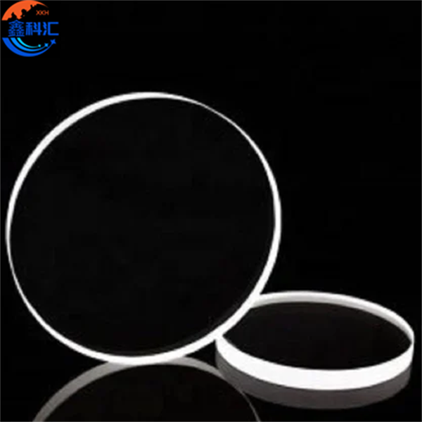
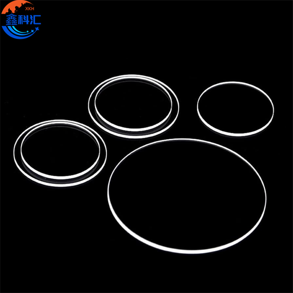
Quartz Glass Wafer JGS1 JGS2 BF33 Wafer 8inch 12inch 725 ± 25 um Or Customized


Specification
| Spec |
4" |
6" |
8" |
10" |
12” |
| Diameter |
100mm |
150mm |
200mm |
250mm |
300mm |
| Thickness |
0.10mm |
0.30mm |
0.40mm |
0.50mm |
0.50mm |
| Primary Flat |
32.5mm |
47.5mm / 57.5mm / Notch |
Notch |
Notch |
Notch |
| LTV (5mmx5mm) |
< 0.5um |
< 0.5um |
< 0.5um |
< 0.5um |
< 0.5um |
| TTV |
< 2um |
< 3um |
<3um |
<10um |
<10um |
| Bow |
±20um |
±30um |
±40um |
±40um |
±40um |
| Warp |
≤ 30um |
≤ 40um |
≤ 70um |
≤ 80um |
≤ 80um |
| Edge Rounding | Compliant with SEMI M1.2 Standard/refer to IEC62276 | ||||
| Surface Type | Single Side Polished / Double Sides Polished | ||||
| Polished side Ra | Ra≤1nm | ||||
| Back Side Criteria | Ra 0.2-0.7um or Customized | ||||
Quartz Glass Wafer JGS1 JGS2 BF33 Wafer parameter table
Application
Quartz glass wafers made from JGS1, JGS2, and BF33 are widely used in various high-precision industries. These wafers are ideal for semiconductor manufacturing, including photomask substrates and wafer-level optics. They are also suitable for optical components, lasers, and sensors in industries such as telecommunications, aerospace, and medical devices. Their high thermal stability and resistance to thermal shock make them perfect for extreme temperature environments, while their exceptional transmittance is crucial for ultraviolet (UV) and infrared (IR) optics.
Properties
Material Types:
JGS1: High UV transmittance, excellent for ultraviolet light applications.
JGS2: Balanced transmittance across UV, visible, and infrared ranges, suitable for general optical uses.
BF33: Borosilicate glass with high chemical resistance and thermal durability.Size Options:
Available in standard sizes of 8-inch and 12-inch wafers.
Custom sizes can be manufactured based on specific requirements.Thickness:
Standard thickness is 725 ± 25 μm.
Customizable thickness available to meet different industrial needs.
Thermal Properties:
Excellent thermal stability, suitable for use in high-temperature environments.
High resistance to thermal shock.
Chemical Resistance:
Strong resistance to corrosion from acids, alkalis, and most chemicals, especially in BF33.
Optical Properties:
JGS1 and JGS2 wafers offer high optical transmittance in ultraviolet (UV), visible, and infrared (IR) ranges.
Ideal for precision optical components, photonics, and laser applications.
Surface Quality:
High surface flatness and smoothness, ensuring precision in semiconductor and optical device manufacturing.
These properties make JGS1, JGS2, and BF33 wafers versatile and reliable for high-performance applications across industries such as optics, electronics, and semiconductors.
Overall
Quartz glass wafers made from JGS1, JGS2, and BF33 offer exceptional performance across a variety of demanding applications. Available in standard sizes of 8-inch and 12-inch with a thickness of 725 ± 25 μm, these wafers are also customizable to meet specific requirements. JGS1 and JGS2 provide high optical transmittance in UV, visible, and IR ranges, while BF33 offers excellent chemical resistance and thermal stability. With high surface flatness and smoothness, these wafers are ideal for precision industries such as semiconductors, optics, and photonics, ensuring reliability and durability in extreme environments and critical applications.
Detailed Diagram