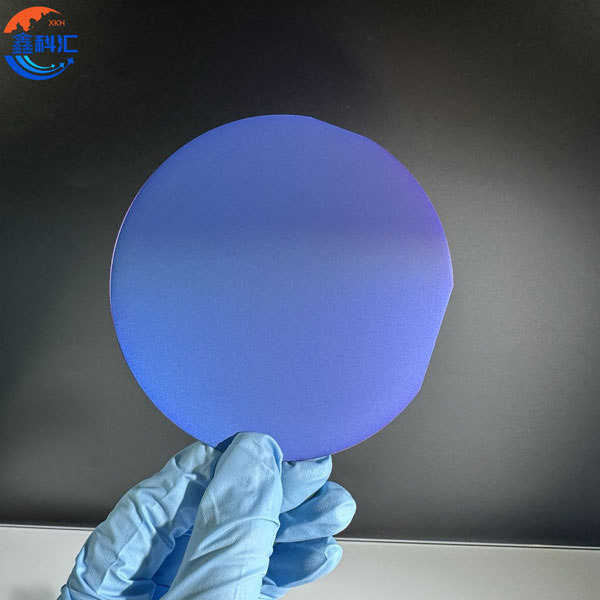
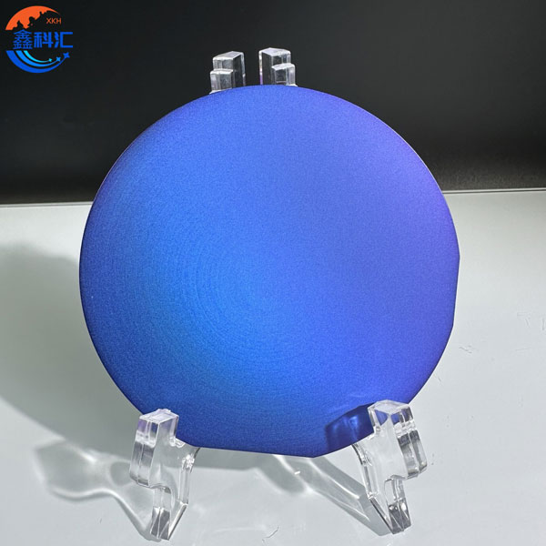
Semi-Insulating SiC on Si Composite Substrates
| Items | Specification | Items | Specification |
| Diameter | 150±0.2mm | Orientation | <111>/<100>/<110> and so on |
| Polytype | 4H | Type | P/N |
| Resistivity | ≥1E8ohm·cm | Flatness | Flat/Notch |
| Transfer layer Thickness | ≥0.1μm | Edge Chip,Scratch,Crack (visual inspection) | None |
| Void | ≤5ea/wafer (2mm>D>0.5mm) | TTV | ≤5μm |
| Front roughness | Ra≤0.2nm (5μm*5μm) |
Thickness | 500/625/675±25μm |
This combination offers a number of advantages in electronics manufacturing:
Compatibility: The use of a silicon substrate makes it compatible with standard silicon-based processing techniques and allows integration with existing semiconductor manufacturing processes.
High temperature performance: SiC has excellent thermal conductivity and can operate at high temperatures, making it suitable for high power and high frequency electronic applications.
High Breakdown Voltage: SiC materials have a high breakdown voltage and can withstand high electric fields without electrical breakdown.
Reduced Power Loss: SiC substrates allow for more efficient power conversion and lower power loss in electronic devices compared to traditional silicon-based materials.
Wide bandwidth: SiC has a wide bandwidth, allowing the development of electronic devices that can operate at higher temperatures and higher power densities.
So semi-insulating SiC on Si composite substrates combines the compatibility of silicon with the superior electrical and thermal properties of SiC, making it suitable for high-performance electronics applications.
Packing and Delivery
1. We will use protective plastic and customized boxed to pack. (Enviroment friendly material)
2. We could do customized packing according to the quantity.
3. DHL/Fedex/UPS Express usually takes about 3-7working days to the destination.
Detailed Diagram


