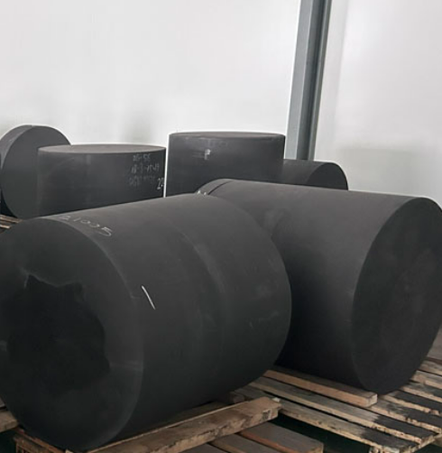
SiC ceramic chuck tray Ceramic suction cups precision machining customized


Material characteristics:
1.High hardness: the Mohs hardness of silicon carbide is 9.2-9.5, second only to diamond, with strong wear resistance.
2. High thermal conductivity: the thermal conductivity of silicon carbide is as high as 120-200 W/m·K, which can dissipate heat quickly and is suitable for high temperature environment.
3. Low thermal expansion coefficient: silicon carbide thermal expansion coefficient is low (4.0-4.5×10⁻⁶/K), can still maintain dimensional stability at high temperature.
4. Chemical stability: silicon carbide acid and alkali corrosion resistance, suitable for use in chemical corrosive environment.
5. High mechanical strength: silicon carbide has high bending strength and compressive strength, and can withstand large mechanical stress.
Features:
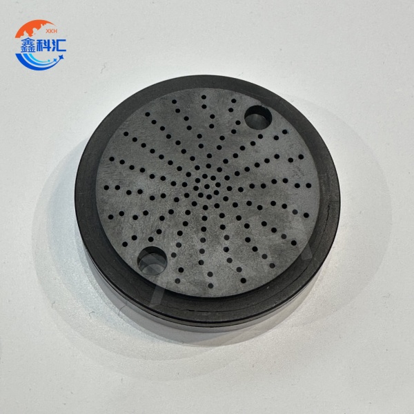
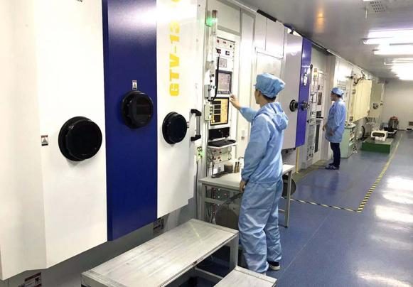
1.In the semiconductor industry, extremely thin wafers need to be placed on a vacuum suction cup, the vacuum suction is used to fix the wafers, and the process of waxing, thinning, waxing, cleaning and cutting is performed on the wafers.
2.Silicon carbide sucker has good thermal conductivity, can effectively shorten the waxing and waxing time, improve production efficiency.
3.Silicon carbide vacuum sucker also has good acid and alkali corrosion resistance.
4.Compared with the traditional corundum carrier plate, shorten the loading and unloading heating and cooling time, improve the work efficiency; At the same time, it can reduce the wear between the upper and lower plates, maintain good plane accuracy, and extend the service life by about 40%.
5.The material proportion is small, light weight. It is easier for operators to carry pallets, reducing the risk of collision damage caused by transport difficulties by about 20%.
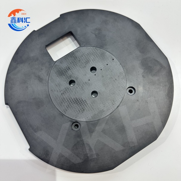
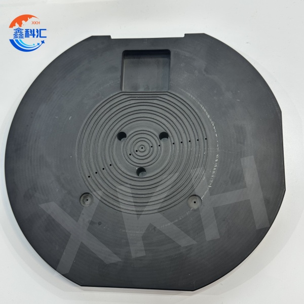
6.Size: maximum diameter 640mm; Flatness: 3um or less
Application field:
1. Semiconductor manufacturing
●Wafer processing:
For wafer fixation in photolithography, etching, thin film deposition and other processes, ensuring high accuracy and process consistency. Its high temperature and corrosion resistance is suitable for harsh semiconductor manufacturing environments.
●Epitaxial growth:
In SiC or GaN epitaxial growth, as a carrier to heat and fix wafers, ensuring temperature uniformity and crystal quality at high temperatures, improving device performance.
2. Photoelectric equipment
●LED Manufacturing:
Used to fix sapphire or SiC substrate, and as a heating carrier in MOCVD process, to ensure the uniformity of epitaxial growth, improve LED luminous efficiency and quality.
●Laser diode:
As a high-precision fixture, fixing and heating substrate to ensure process temperature stability, improve the output power and reliability of the laser diode.
3. Precision machining
●Optical component processing:
It is used for fixing precision components such as optical lenses and filters to ensure high precision and low pollution during processing, and is suitable for high-intensity machining.
●Ceramic processing:
As a high stability fixture, it is suitable for precision machining of ceramic materials to ensure machining accuracy and consistency under high temperature and corrosive environment.
4. Scientific experiments
●High temperature experiment:
As a sample fixation device in high temperature environments, it supports extreme temperature experiments above 1600°C to ensure temperature uniformity and sample stability.
●Vacuum test:
As a sample fixing and heating carrier in vacuum environment, to ensure the accuracy and repeatability of the experiment, suitable for vacuum coating and heat treatment.
Technical specifications:
|
(Material property) |
(Unit) |
(ssic) |
|
|
(SiC content) |
|
(Wt)% |
>99 |
|
(Average grain size) |
|
micron |
4-10 |
|
(Density) |
|
kg/dm3 |
>3.14 |
|
(Apparent porosity) |
|
Vo1% |
<0.5 |
|
(Vickers hardness) |
HV 0.5 |
GPa |
28 |
|
*( Flexural strength) |
20ºC |
MPa |
450 |
|
(Compressive strength) |
20ºC |
MPa |
3900 |
|
(Elastic Modulus) |
20ºC |
GPa |
420 |
|
(Fracture toughness) |
|
MPa/m'% |
3.5 |
|
(Thermal conductivity) |
20°ºC |
W/(m*K) |
160 |
|
(Resistivity) |
20°ºC |
Ohm.cm |
106-108 |
|
|
a(RT**...80ºC) |
K-1*10-6 |
4.3 |
|
|
|
oºC |
1700 |
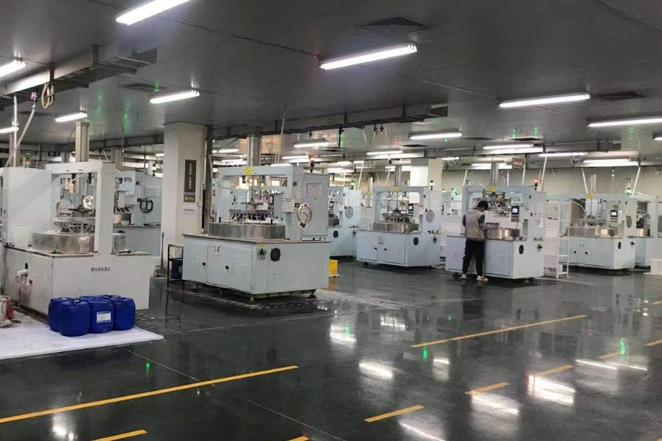
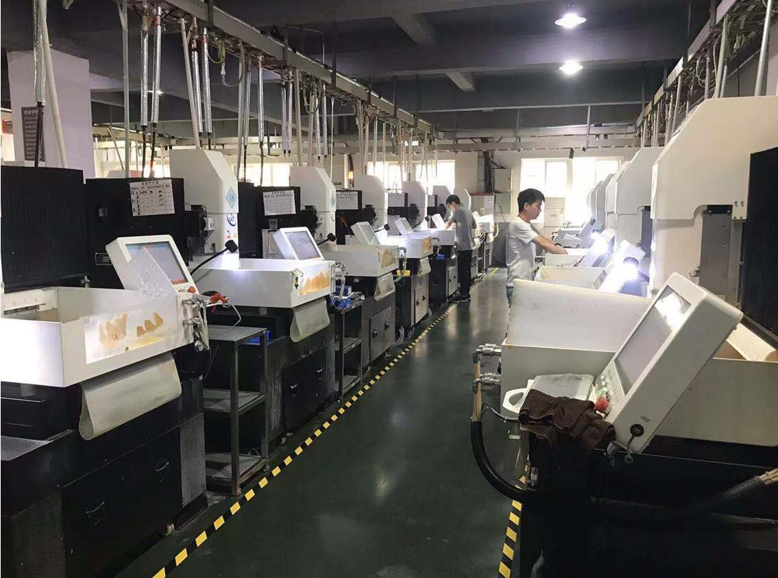
With years of technical accumulation and industry experience, XKH is able to tailor key parameters such as the size, heating method and vacuum adsorption design of the chuck according to the specific needs of the customer, ensuring that the product is perfectly adapted to the customer's process. SiC silicon carbide ceramic chucks have become indispensable components in wafer processing, epitaxial growth and other key processes due to their excellent thermal conductivity, high temperature stability and chemical stability. Especially in the manufacturing of third-generation semiconductor materials such as SiC and GaN, the demand for silicon carbide ceramic chucks continues to grow. In the future, with the rapid development of 5G, electric vehicles, artificial intelligence and other technologies, the application prospects of silicon carbide ceramic chucks in the semiconductor industry will be broader.
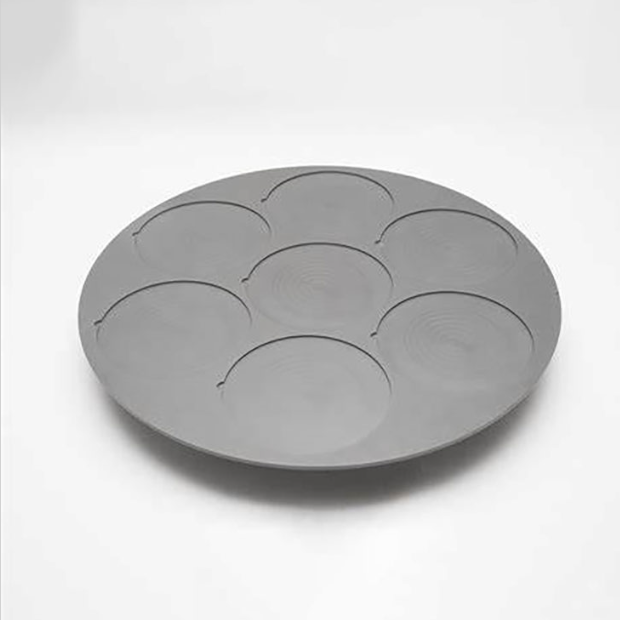
Detailed Diagram