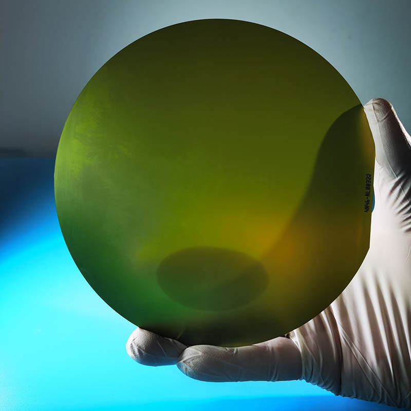
SiC wafer 4H-N 6H-N HPSI 4H-semi 6H-semi 4H-P 6H-P 3C type 2inch 3inch 4inch 6inch 8inch
Properties
4H-N and 6H-N (N-type SiC Wafers)
Application: Primarily used in power electronics, optoelectronics, and high-temperature applications.
Diameter Range: 50.8 mm to 200 mm.
Thickness: 350 μm ± 25 μm, with optional thicknesses of 500 μm ± 25 μm.
Resistivity: N-type 4H/6H-P: ≤ 0.1 Ω·cm (Z-grade), ≤ 0.3 Ω·cm (P-grade); N-type 3C-N: ≤ 0.8 mΩ·cm (Z-grade), ≤ 1 mΩ·cm (P-grade).
Roughness: Ra ≤ 0.2 nm (CMP or MP).
Micropipe Density (MPD): < 1 ea/cm².
TTV: ≤ 10 μm for all diameters.
Warp: ≤ 30 μm (≤ 45 μm for 8-inch wafers).
Edge Exclusion: 3 mm to 6 mm depending on wafer type.
Packaging: Multi-wafer cassette or single wafer container.
Ohter available size 3inch 4inch 6inch 8inch
HPSI (High Purity Semi-Insulating SiC Wafers)
Application: Used for devices requiring high resistance and stable performance, such as RF devices, photonic applications, and sensors.
Diameter Range: 50.8 mm to 200 mm.
Thickness: Standard thickness of 350 μm ± 25 μm with options for thicker wafers up to 500 μm.
Roughness: Ra ≤ 0.2 nm.
Micropipe Density (MPD): ≤ 1 ea/cm².
Resistivity: High resistance, typically used in semi-insulating applications.
Warp: ≤ 30 μm (for smaller sizes), ≤ 45 μm for larger diameters.
TTV: ≤ 10 μm.
Ohter available size 3inch 4inch 6inch 8inch
4H-P、 6H-P &3C SiC wafer (P-type SiC Wafers)
Application: Primarily for power and high-frequency devices.
Diameter Range: 50.8 mm to 200 mm.
Thickness: 350 μm ± 25 μm or customized options.
Resistivity: P-type 4H/6H-P: ≤ 0.1 Ω·cm (Z-grade), ≤ 0.3 Ω·cm (P-grade).
Roughness: Ra ≤ 0.2 nm (CMP or MP).
Micropipe Density (MPD): < 1 ea/cm².
TTV: ≤ 10 μm.
Edge Exclusion: 3 mm to 6 mm.
Warp: ≤ 30 μm for smaller sizes, ≤ 45 μm for larger sizes.
Ohter available size 3inch 4inch 6inch 5×5 10×10
Partial Data Parameters Table
|
Property |
2 inch |
3inch |
4inch |
6inch |
8inch |
|||
|
Type |
4H-N/HPSI/ |
4H-N/HPSI/ |
4H-N/HPSI//4H/6H-P/3C; |
4H-N/HPSI//4H/6H-P/3C; |
4H-N/HPSI/4H-SEMI |
|||
|
Diameter |
50.8 ± 0.3 mm |
76.2±0.3mm |
100±0.3mm |
150±0.3mm |
200 ± 0.3 mm |
|||
|
Thickness |
330 ± 25 um |
350 ±25 um |
350 ±25 um |
350 ±25 um |
350 ±25 um |
|||
|
350±25um; |
500±25um |
500±25um |
500±25um |
500±25um |
||||
|
or customized |
or customized |
or customized |
or customized |
or customized |
||||
|
Roughness |
Ra ≤ 0.2nm |
Ra ≤ 0.2nm |
Ra ≤ 0.2nm |
Ra ≤ 0.2nm |
Ra ≤ 0.2nm |
|||
|
Warp |
≤ 30um |
≤ 30um |
≤ 30um |
≤ 30um |
≤45um |
|||
|
TTV |
≤ 10um |
≤ 10um |
≤ 10um |
≤ 10um |
≤ 10um |
|||
|
Scratch/Dig |
CMP/MP |
|||||||
|
MPD |
<1ea/cm-2 |
<1ea/cm-2 |
<1ea/cm-2 |
<1ea/cm-2 |
<1ea/cm-2 |
|||
|
Shape |
Round, Flat 16mm;OF length 22mm ; OF Length 30/32.5mm; OF Length47.5mm; NOTCH; NOTCH; |
|||||||
|
Bevel |
45°, SEMI Spec; C Shape |
|||||||
|
Grade |
Production grade for MOS&SBD; Research grade ; Dummy grade ,Seed wafer Grade |
|||||||
|
Remarks |
Diameter, Thickness, Orientation, specifications above can be customized upon your request |
|||||||
Applications
· Power Electronics
N type SiC wafers are crucial in power electronic devices due to their ability to handle high voltage and high current. They are commonly used in power converters, inverters, and motor drives for industries like renewable energy, electric vehicles, and industrial automation.
· Optoelectronics
N type SiC materials, especially for optoelectronic applications, are employed in devices such as light-emitting diodes (LEDs) and laser diodes. Their high thermal conductivity and wide bandgap make them ideal for high-performance optoelectronic devices.
· High-Temperature Applications
4H-N 6H-N SiC wafers are well-suited for high-temperature environments, such as in sensors and power devices used in aerospace, automotive, and industrial applications where heat dissipation and stability at elevated temperatures are critical.
· RF Devices
4H-N 6H-N SiC wafers are used in radio frequency (RF) devices that operate in high-frequency ranges. They are applied in communication systems, radar technology, and satellite communications, where high power efficiency and performance are required.
· Photonic Applications
In photonics, SiC wafers are used for devices like photodetectors and modulators. The material's unique properties allow it to be effective in light generation, modulation, and detection in optical communication systems and imaging devices.
· Sensors
SiC wafers are used in a variety of sensor applications, particularly in harsh environments where other materials might fail. These include temperature, pressure, and chemical sensors, which are essential in fields like automotive, oil & gas, and environmental monitoring.
· Electric Vehicle Drive Systems
SiC technology plays a significant role in electric vehicles by improving the efficiency and performance of the drive systems. With SiC power semiconductors, electric vehicles can achieve better battery life, faster charging times, and greater energy efficiency.
· Advanced Sensors and Photonic Converters
In advanced sensor technologies, SiC wafers are used for creating high-precision sensors for applications in robotics, medical devices, and environmental monitoring. In photonic converters, SiC’s properties are exploited to enable efficient conversion of electrical energy to optical signals, which is vital in telecommunications and high-speed internet infrastructure.
Q&A
Q:What is 4H in 4H SiC?
A:"4H" in 4H SiC refers to the crystal structure of silicon carbide, specifically a hexagonal form with four layers (H). The "H" indicates the type of hexagonal polytype, distinguishing it from other SiC polytypes like 6H or 3C.
Q:What is the thermal conductivity of 4H-SiC?
A:The thermal conductivity of 4H-SiC (Silicon Carbide) is approximately 490-500 W/m·K at room temperature. This high thermal conductivity makes it ideal for applications in power electronics and high-temperature environments, where efficient heat dissipation is crucial.


