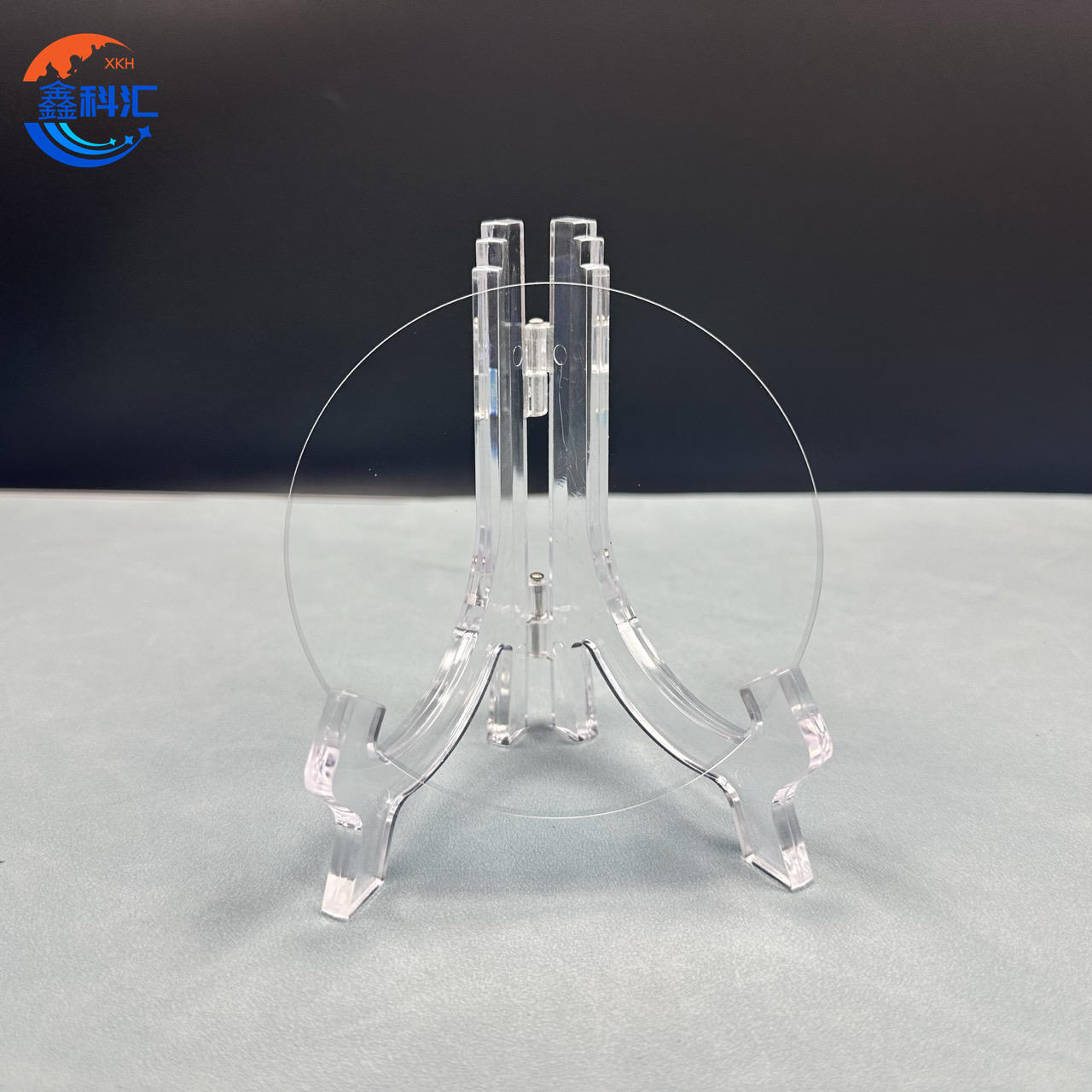
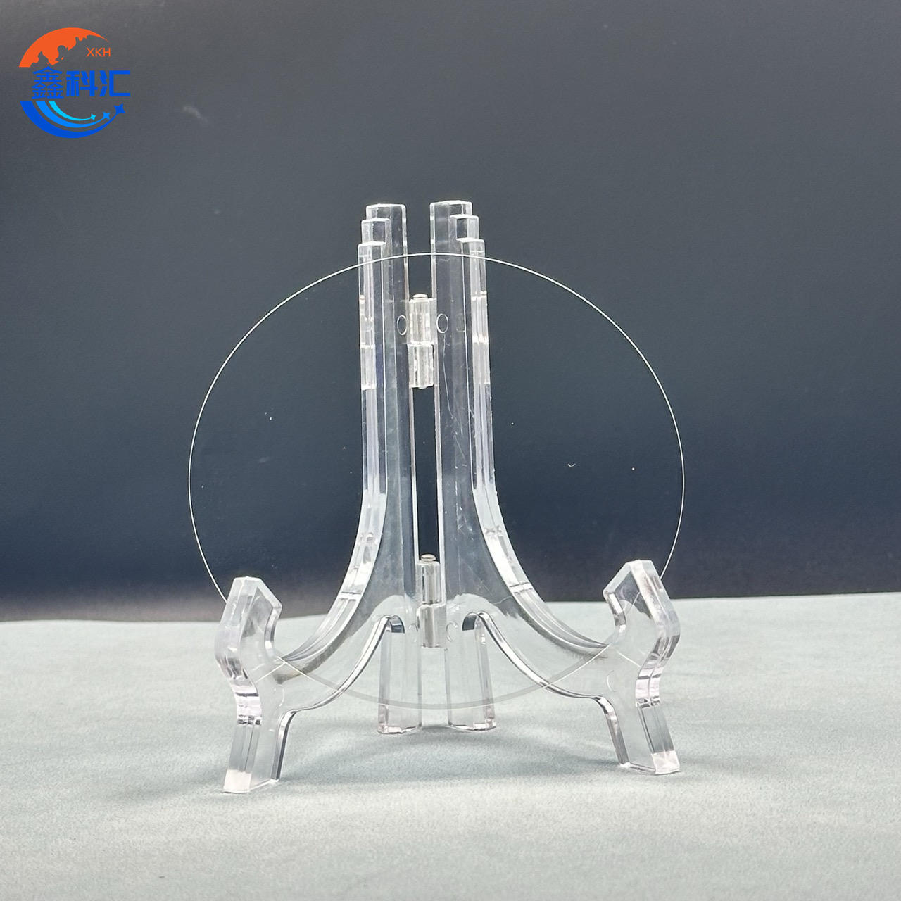
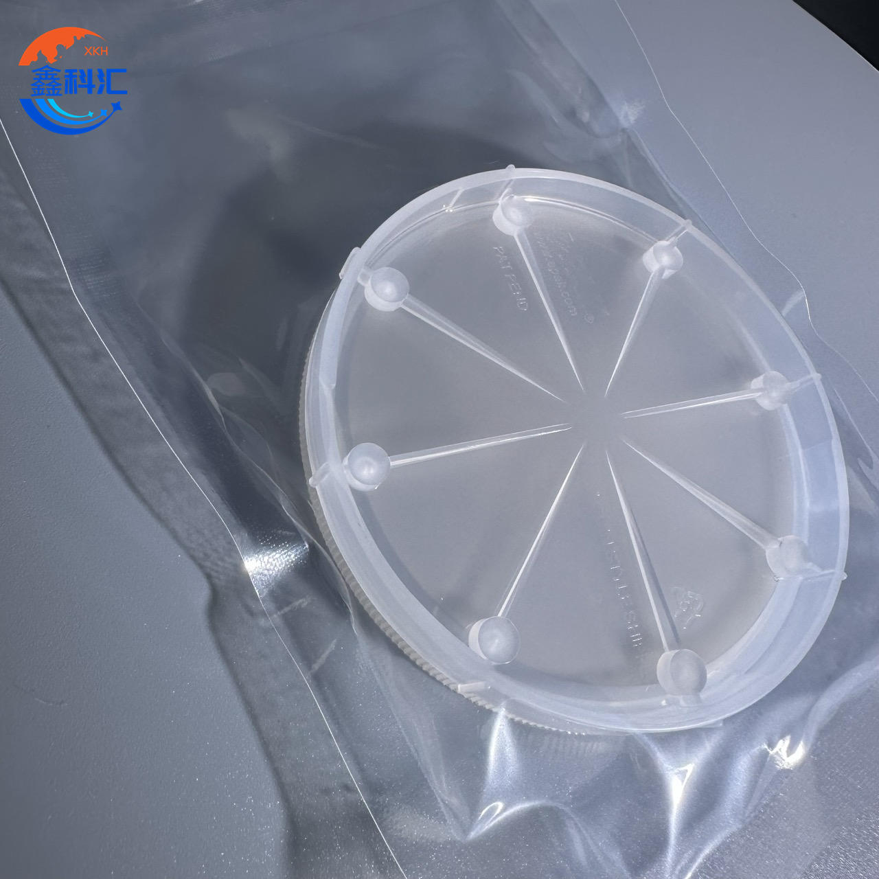
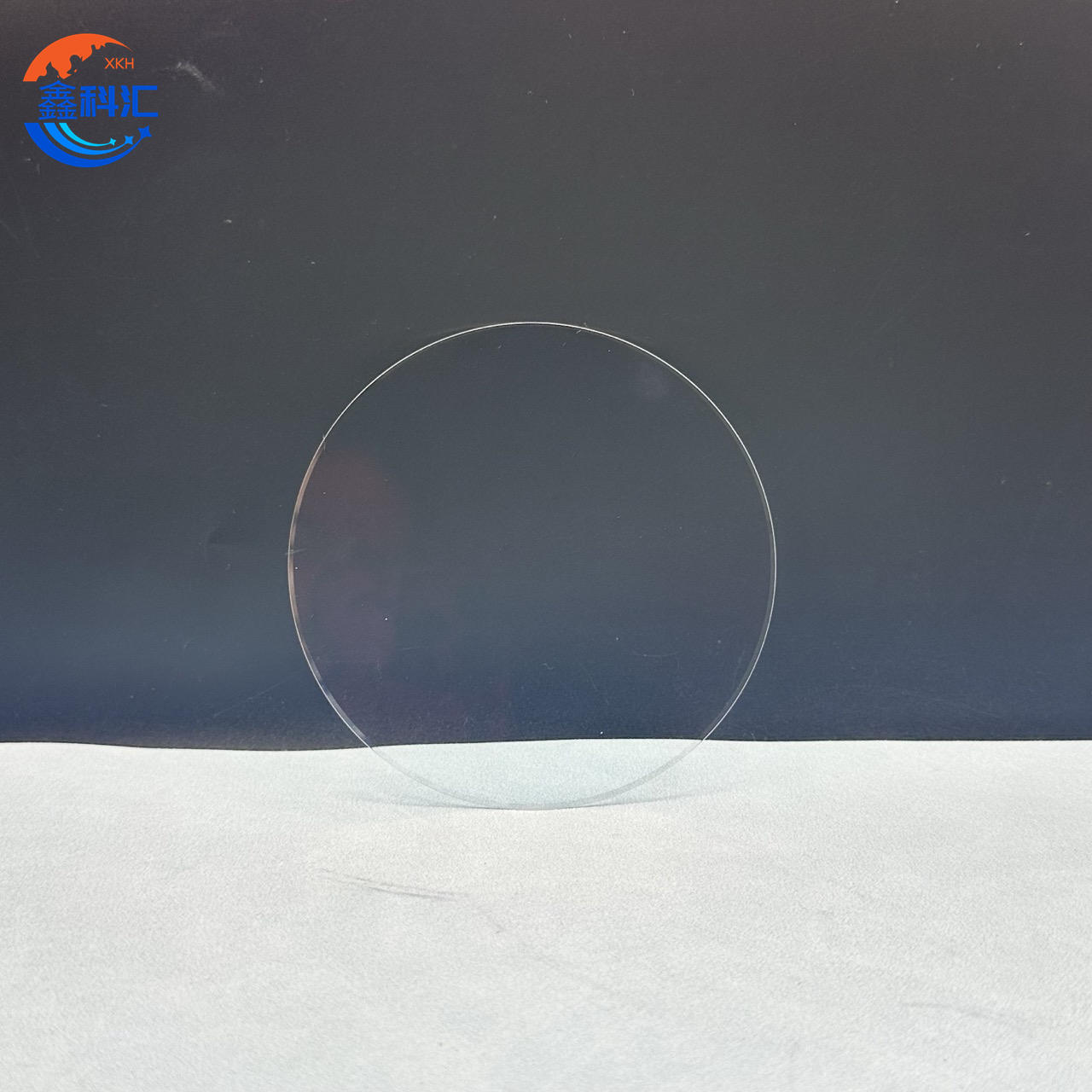
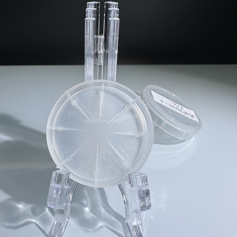
SiC substrate 3inch 350um thickness HPSI type Prime Grade Dummy grade
Properties
|
Parameter |
Production Grade |
Research Grade |
Dummy Grade |
Unit |
| Grade | Production Grade | Research Grade | Dummy Grade | |
| Diameter | 76.2 ± 0.5 | 76.2 ± 0.5 | 76.2 ± 0.5 | mm |
| Thickness | 500 ± 25 | 500 ± 25 | 500 ± 25 | µm |
| Wafer Orientation | On-axis: <0001> ± 0.5° | On-axis: <0001> ± 2.0° | On-axis: <0001> ± 2.0° | degree |
| Micropipe Density (MPD) | ≤ 1 | ≤ 5 | ≤ 10 | cm−2^-2−2 |
| Electrical Resistivity | ≥ 1E10 | ≥ 1E5 | ≥ 1E5 | Ω·cm |
| Dopant | Undoped | Undoped | Undoped | |
| Primary Flat Orientation | {1-100} ± 5.0° | {1-100} ± 5.0° | {1-100} ± 5.0° | degree |
| Primary Flat Length | 32.5 ± 3.0 | 32.5 ± 3.0 | 32.5 ± 3.0 | mm |
| Secondary Flat Length | 18.0 ± 2.0 | 18.0 ± 2.0 | 18.0 ± 2.0 | mm |
| Secondary Flat Orientation | 90° CW from primary flat ± 5.0° | 90° CW from primary flat ± 5.0° | 90° CW from primary flat ± 5.0° | degree |
| Edge Exclusion | 3 | 3 | 3 | mm |
| LTV/TTV/Bow/Warp | 3 / 10 / ±30 / 40 | 3 / 10 / ±30 / 40 | 5 / 15 / ±40 / 45 | µm |
| Surface Roughness | Si-face: CMP, C-face: Polished | Si-face: CMP, C-face: Polished | Si-face: CMP, C-face: Polished | |
| Cracks (High-Intensity Light) | None | None | None | |
| Hex Plates (High-Intensity Light) | None | None | Cumulative area 10% | % |
| Polytype Areas (High-Intensity Light) | Cumulative area 5% | Cumulative area 20% | Cumulative area 30% | % |
| Scratches (High-Intensity Light) | ≤ 5 scratches, cumulative length ≤ 150 | ≤ 10 scratches, cumulative length ≤ 200 | ≤ 10 scratches, cumulative length ≤ 200 | mm |
| Edge Chipping | None ≥ 0.5 mm width/depth | 2 allowed ≤ 1 mm width/depth | 5 allowed ≤ 5 mm width/depth | mm |
| Surface Contamination | None | None | None |
Applications
1. High-Power Electronics
The superior thermal conductivity and wide bandgap of SiC wafers make them ideal for high-power, high-frequency devices:
●MOSFETs and IGBTs for power conversion.
●Advanced electric vehicle power systems, including inverters and chargers.
●Smart grid infrastructure and renewable energy systems.
2. RF and Microwave Systems
SiC substrates enable high-frequency RF and microwave applications with minimal signal loss:
●Telecommunications and satellite systems.
●Aerospace radar systems.
●Advanced 5G network components.
3. Optoelectronics and Sensors
The unique properties of SiC support a variety of optoelectronic applications:
●UV detectors for environmental monitoring and industrial sensing.
●LED and laser substrates for solid-state lighting and precision instruments.
●High-temperature sensors for aerospace and automotive industries.
4. Research and Development
The diversity of grades (Production, Research, Dummy) enables cutting-edge experimentation and device prototyping in academia and industry.
Advantages
●Reliability: Excellent resistivity and stability across grades.
●Customization: Tailored orientations and thicknesses to suit different needs.
●High Purity: Undoped composition ensures minimal impurity-related variations.
●Scalability: Meets the requirements of both mass production and experimental research.
The 3-inch high-purity SiC wafers are your gateway to high-performance devices and innovative technological advancements. For inquiries and detailed specifications, contact us today.
Summary
The 3-inch High Purity Silicon Carbide (SiC) Wafers, available in Production, Research, and Dummy Grades, are premium substrates designed for high-power electronics, RF/microwave systems, optoelectronics, and advanced R&D. These wafers feature undoped, semi-insulating properties with excellent resistivity (≥1E10 Ω·cm for Production Grade), low micropipe density (≤1 cm−2^-2−2), and exceptional surface quality. They are optimized for high-performance applications, including power conversion, telecommunications, UV sensing, and LED technologies. With customizable orientations, superior thermal conductivity, and robust mechanical properties, these SiC wafers enable efficient, reliable device fabrication and groundbreaking innovations across industries.
Detailed Diagram
