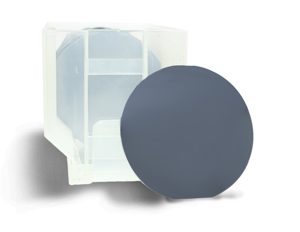
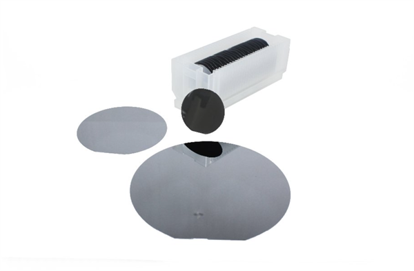
SiC substrate P-type 4H/6H-P 3C-N 4inch withe thickness of 350um Production grade Dummy grade


4inch SiC substrate P-type 4H/6H-P 3C-N parameter table
4 inch diameter Silicon Carbide (SiC) Substrate Specification
| Grade | Zero MPD Production
Grade (Z Grade) |
Standard Production
Grade (P Grade) |
Dummy Grade (D Grade) |
||
| Diameter | 99.5 mm~100.0 mm | ||||
| Thickness | 350 μm ± 25 μm | ||||
| Wafer Orientation | Off axis: 2.0°-4.0°toward [1120] ± 0.5° for 4H/6H-P, On axis:〈111〉± 0.5° for 3C-N | ||||
| Micropipe Density | 0 cm-2 | ||||
| Resistivity | p-type 4H/6H-P | ≤0.1 Ωꞏcm | ≤0.3 Ωꞏcm | ||
| n-type 3C-N | ≤0.8 mΩꞏcm | ≤1 m Ωꞏcm | |||
| Primary Flat Orientation | 4H/6H-P | -
{1010} ± 5.0° |
|||
| 3C-N | -
{110} ± 5.0° |
||||
| Primary Flat Length | 32.5 mm ± 2.0 mm | ||||
| Secondary Flat Length | 18.0 mm ± 2.0 mm | ||||
| Secondary Flat Orientation | Silicon face up: 90° CW. from Prime flat ± 5.0° | ||||
| Edge Exclusion | 3 mm | 6 mm | |||
| LTV/TTV/Bow /Warp | ≤2.5 μm/≤5 μm/≤15 μm/≤30 μm | ≤10 μm/≤15 μm/≤25 μm/≤40 μm | |||
| Roughness | Polish Ra≤1 nm | ||||
| CMP Ra≤0.2 nm | Ra≤0.5 nm | ||||
| Edge Cracks By High Intensity Light | None | Cumulative length ≤ 10 mm, single length≤2 mm | |||
| Hex Plates By High Intensity Light | Cumulative area ≤0.05% | Cumulative area ≤0.1% | |||
| Polytype Areas By High Intensity Light | None | Cumulative area≤3% | |||
| Visual Carbon Inclusions | Cumulative area ≤0.05% | Cumulative area ≤3% | |||
| Silicon Surface Scratches By High Intensity Light | None | Cumulative length≤1×wafer diameter | |||
| Edge Chips High By Intensity Light | None permitted ≥0.2mm width and depth | 5 allowed, ≤1 mm each | |||
| Silicon Surface Contamination By High Intensity | None | ||||
| Packaging | Multi-wafer Cassette or Single Wafer Container | ||||
Notes:
※Defects limits apply to entire wafer surface except for the edge exclusion area. # The scratches should be checked on Si face only.
The P-type 4H/6H-P 3C-N 4-inch SiC substrate with a thickness of 350 μm is widely applied in advanced electronic and power device manufacturing. With excellent thermal conductivity, high breakdown voltage, and strong resistance to extreme environments, this substrate is ideal for high-performance power electronics such as high-voltage switches, inverters, and RF devices. Production-grade substrates are used in large-scale manufacturing, ensuring reliable, high-precision device performance, which is critical for power electronics and high-frequency applications. Dummy-grade substrates, on the other hand, are mainly used for process calibration, equipment testing, and prototype development, helping maintain quality control and process consistency in semiconductor production.
SpecificationThe advantages of N-type SiC composite substrates include
- High Thermal Conductivity: Efficient heat dissipation makes the substrate ideal for high-temperature and high-power applications.
- High Breakdown Voltage: Supports high-voltage operation, ensuring reliability in power electronics and RF devices.
- Resistance to Harsh Environments: Durable in extreme conditions such as high temperatures and corrosive environments, ensuring long-lasting performance.
- Production-Grade Precision: Ensures high-quality and reliable performance in large-scale manufacturing, suitable for advanced power and RF applications.
- Dummy-Grade for Testing: Enables accurate process calibration, equipment testing, and prototyping without compromising production-grade wafers.
Overall, the P-type 4H/6H-P 3C-N 4-inch SiC substrate with a thickness of 350 μm offers significant advantages for high-performance electronic applications. Its high thermal conductivity and breakdown voltage make it ideal for high-power and high-temperature environments, while its resistance to harsh conditions ensures durability and reliability. The production-grade substrate ensures precise and consistent performance in large-scale manufacturing of power electronics and RF devices. Meanwhile, the dummy-grade substrate is essential for process calibration, equipment testing, and prototyping, supporting quality control and consistency in semiconductor production. These features make SiC substrates highly versatile for advanced applications.
Detailed Diagram