Silicon carbide ceramic tray sucker Silicon carbide ceramic tube supply high temperature sintering custom processing
Main features:
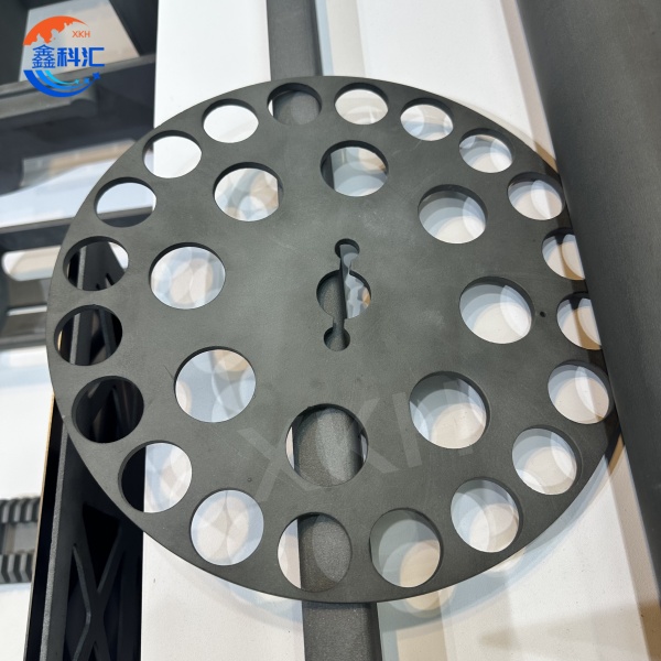
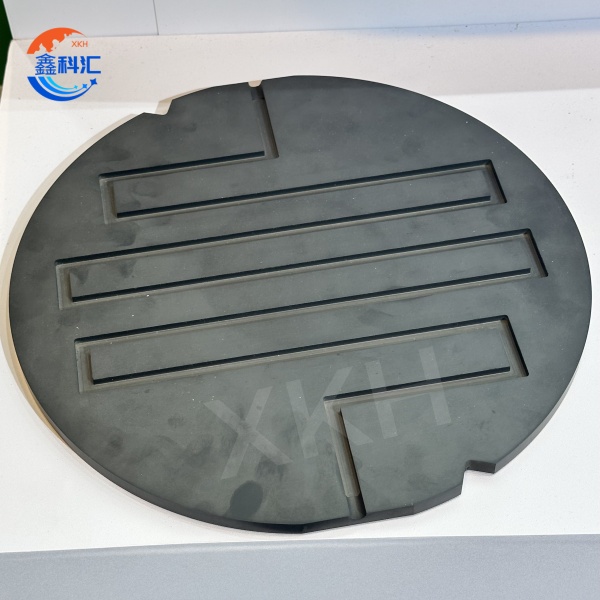
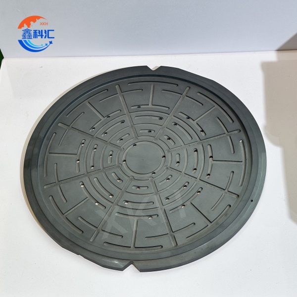
1. Silicon carbide ceramic tray
- High hardness and wear resistance: the hardness is close to diamond, and can withstand mechanical wear in wafer processing for a long time.
- High thermal conductivity and low thermal expansion coefficient: fast heat dissipation and dimensional stability, avoiding deformation caused by thermal stress.
- High flatness and surface finish: The surface flatness is up to the micron level, ensuring full contact between the wafer and the disk, reducing contamination and damage.
Chemical stability: Strong corrosion resistance, suitable for wet cleaning and etching processes in semiconductor manufacturing.
2. Silicon carbide ceramic tube
- High temperature resistance: It can work in high temperature environment above 1600°C for a long time, suitable for semiconductor high temperature process.
Excellent corrosion resistance: resistant to acids, alkalis and a variety of chemical solvents, suitable for harsh process environments.
- High hardness and wear resistance: resist particle erosion and mechanical wear, extend service life.
- High thermal conductivity and low coefficient of thermal expansion: fast conduction of heat and dimensional stability, reducing deformation or cracking caused by thermal stress.
Product Parameter:
Silicon carbide ceramic tray parameter:
| (Material property) | (Unit) | (ssic) | |
| (SiC content) | (Wt)% | >99 | |
| (Average grain size) | micron | 4-10 | |
| (Density) | kg/dm3 | >3.14 | |
| (Apparent porosity) | Vo1% | <0.5 | |
| (Vickers hardness) | HV 0.5 | GPa | 28 |
| *() Flexural strength* (three points) |
20ºC | MPa | 450 |
| (Compressive strength) | 20ºC | MPa | 3900 |
| (Elastic Modulus) | 20ºC | GPa | 420 |
| (Fracture toughness) | MPa/m'% | 3.5 | |
| (Thermal conductivity) | 20°ºC | W/(m*K) | 160 |
| (Resistivity) | 20°ºC | Ohm.cm | 106-108 |
(Thermal expansion coefficient) |
a(RT**...80ºC) | K-1*10-6 | 4.3 |
(Maximum operating temperature) |
oºC | 1700 | |
Silicon carbide ceramic tube parameter:
| Items | Index |
| α-SIC | 99% min |
| Apparent Porosity | 16% max |
| Bulk Density | 2.7g/cm3 min |
| Bending Strength at High Temperature | 100 Mpa min |
| Coefficient of Thermal Expansion | K-1 4.7x10 -6 |
| Coefficient of Thermal Conductivity(1400ºC) | 24 W/m.k |
| Max. Working Temperature | 1650ºC |
Main applications:
1. Silicon carbide ceramic plate
- Wafer cutting and polishing: serves as a bearing platform to ensure high precision and stability during cutting and polishing.
- Lithography process: The wafer is fixed in the lithography machine to ensure high precision positioning during exposure.
- Chemical Mechanical Polishing (CMP) : acts as a support platform for polishing pads, providing uniform pressure and heat distribution.
2. Silicon carbide ceramic tube
- High temperature furnace tube: used for high temperature equipment such as diffusion furnace and oxidation furnace to carry wafers for high temperature process treatment.
- CVD/PVD process: As a bearing tube in the reaction chamber, resistant to high temperatures and corrosive gases.
- Semiconductor equipment accessories: for heat exchangers, gas pipelines, etc., to improve the thermal management efficiency of equipment.
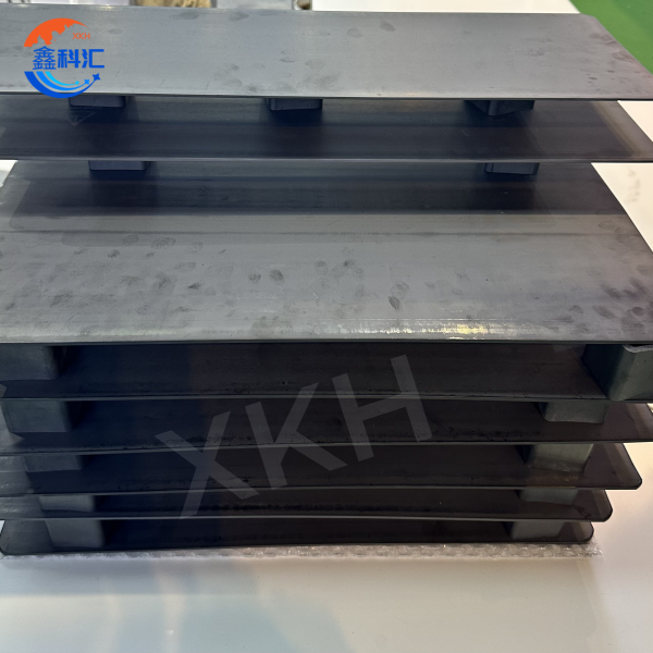
XKH offers a full range of custom services for silicon carbide ceramic trays, suction cups and silicon carbide ceramic tubes. Silicon carbide ceramic trays and suction cups, XKH can be customized according to customer requirements of different sizes, shapes and surface roughness, and support special coating treatment, enhance wear resistance and corrosion resistance; For silicon carbide ceramic tubes, XKH can customize a variety of inner diameter, outer diameter, length and complex structure (such as shaped tube or porous tube), and provide polishing, anti-oxidation coating and other surface treatment processes. XKH ensures that customers can take full advantage of the performance benefits of silicon carbide ceramic products to meet the demanding requirements of high-end manufacturing fields such as semiconductors, leds and photovoltaics.
Detailed Diagram


